Method for detecting photoresist damage using dark field silicon wafer inspection machine

A technology for detecting light and detectors, applied in semiconductor/solid-state device testing/measurement, electrical components, circuits, etc., can solve problems such as time-consuming and labor-intensive, inability to accurately reflect the degree of photoresist damage in real time, and avoid production losses , damage prevention, the effect of real-time scanning

Active Publication Date: 2017-01-11
SHANGHAI HUALI MICROELECTRONICS CORP
View PDF5 Cites 0 Cited by
  • Summary
  • Abstract
  • Description
  • Claims
  • Application Information

AI Technical Summary

Problems solved by technology

[0009] The present invention solves the problem that the existing photoresist damage detection method is time-consuming and labor-intensive and cannot accurately and real-time reflect the damage degree of the photoresist when the machine actually scans the product, thereby providing a dark-field silicon wafer detection machine to detect the photoresist Damaged approach to technical solutions

Method used


Image

  • Method for detecting photoresist damage using dark field silicon wafer inspection machine
  • Method for detecting photoresist damage using dark field silicon wafer inspection machine
  • Method for detecting photoresist damage using dark field silicon wafer inspection machine

Examples


Embodiment Construction

[0029] The present invention will be further described below in conjunction with the accompanying drawings and specific embodiments, but not as a limitation of the present invention.

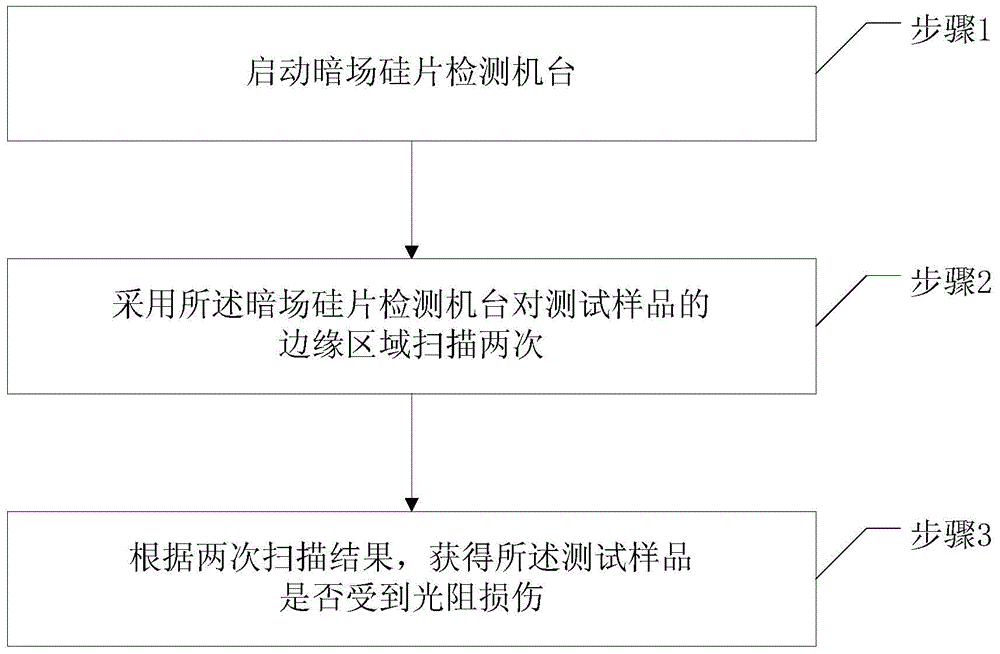
[0030] like figure 1 and figure 2 As shown, the present invention provides a method for detecting photoresist damage using a dark-field silicon wafer detection machine, comprising the following steps:

[0031] Step 1. The user first sets the scanning program of the dark field wafer inspection machine according to the relevant parameters of the sample to be tested (wafer with photoresist), and starts the dark field wafer inspection machine;

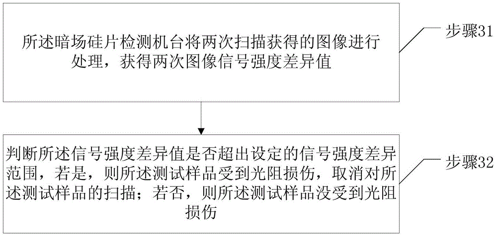
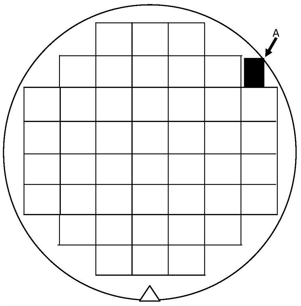
[0032] Step 2. Use the dark field silicon wafer detection machine to test the edge area A of the sample (such as Figure 3 to Figure 5 Shown) scan twice, the edge area of ​​the test sample is selected because the incomplete product does not affect the yield rate, and it can ensure that if the photoresist damage is caused to the test sample during the dete...


PUM


Abstract

The invention discloses a method for detecting photoresist damage through a dark-field silicon wafer detection machine, and relates to the field of integrated circuit manufacturing. The method comprises the steps that the dark-field silicon wafer detection machine is started; the edge areas of a test sample are scanned twice through the dark-field silicon wafer detection machine; according to two scanning results, it is determined whether the test sample is subject to the photoresist damage. According to the method, whether the test sample is subject to the photoresist damage is determined by scanning the edge areas of the test sample twice in advance, real-time scanning is achieved, and the degree of photoresist damage caused in the process of actually scanning a product by the machine can be accurately reflected. In addition, the damage which may be caused can be prevented in advance according to the detection results, and therefore production loss can be avoided in time.

Description

technical field [0001] The invention relates to the field of integrated circuit manufacturing, in particular to a method for detecting photoresist damage. Background technique [0002] Photoresist is a kind of photosensitive material. Different photoresists will change their chemical properties after being exposed to a specific wavelength light source, and then through the action of the developer, the photoresist can form the pattern required for the process. Sensitivity makes it possible to cause photoresist damage due to changes in properties or shapes when exposed to other light sources during the production process. At present, product inspection machines in semiconductor manufacturing plants generally have light source irradiation during the inspection process. Therefore, in the inspection zone There is a risk of photoresist damage when using photoresist products. [0003] Some dark-field silicon wafer inspection machines use a laser with a wavelength of 355nm as the l...

Claims


Application Information

Patent Timeline
Patent Type & Authority Patents(China)
IPC IPC(8): H01L21/66
CPCH01L22/24
Inventor 何广智龙吟倪棋梁陈宏璘
Owner SHANGHAI HUALI MICROELECTRONICS CORP
Why Eureka
Try Eureka