Manufacturing method of solar cell and solar cell

A technology for a solar cell and a manufacturing method, applied in the field of solar cells, can solve the problems of increased processes, increased manufacturing costs, different substrates, etc., and achieves the effects of shortening the annealing treatment time, shortening the annealing treatment time, and improving mass productivity.

Active Publication Date: 2016-09-21
ULVAC INC
View PDF5 Cites 0 Cited by
  • Summary
  • Abstract
  • Description
  • Claims
  • Application Information

AI Technical Summary

Problems solved by technology

According to this, alignment can be performed with an accuracy of 50 μm or less, but the process of forming an alignment mark is increased, and as a result, there is a problem of increasing the manufacturing cost that is most desired to be avoided.
[0012] Furthermore, as an external specification, in addition to 156mm on one side, there is also an external specification of approximately 125mm on one side, and when alignment is performed based on the periphery of the substrate, there is a problem that it cannot handle substrates with different processing positions.

Method used


Image

  • Manufacturing method of solar cell and solar cell
  • Manufacturing method of solar cell and solar cell
  • Manufacturing method of solar cell and solar cell

Examples


Embodiment Construction

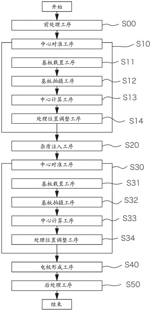
[0060] Hereinafter, an embodiment of a method for manufacturing a solar cell according to the present invention will be described with reference to the drawings.

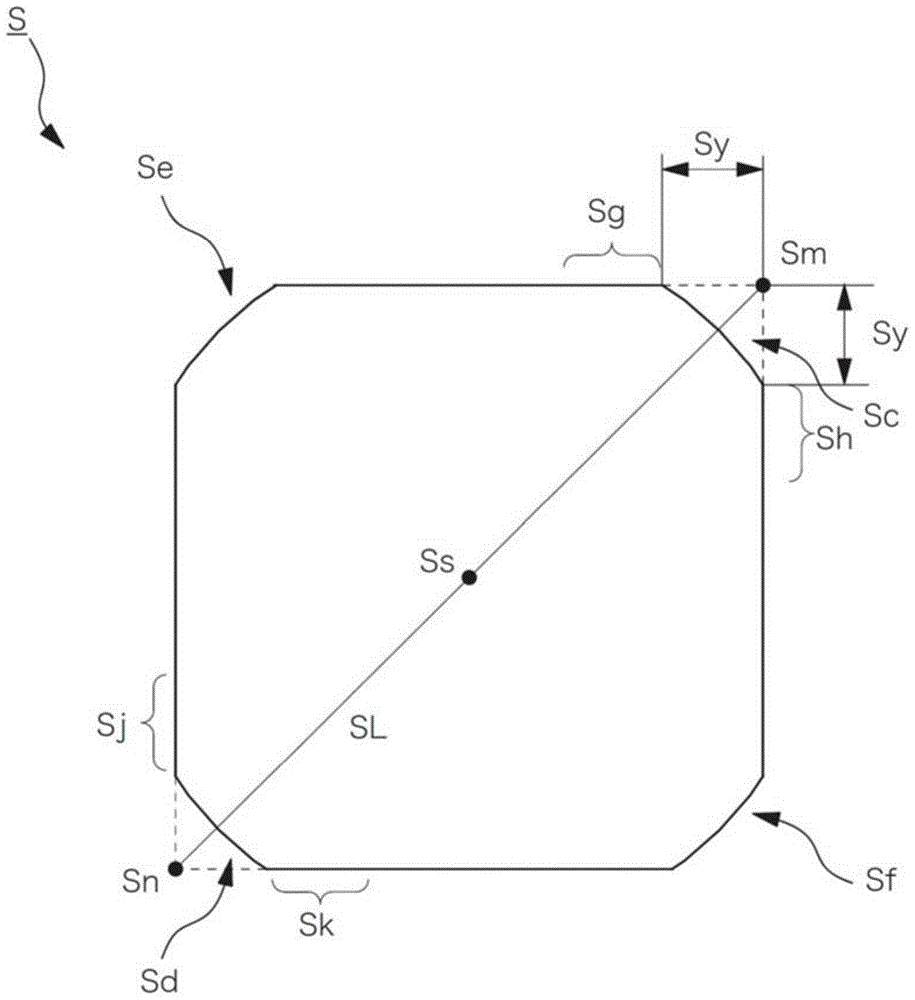
[0061] figure 1 It is a top view showing the solar cell substrate in this embodiment, figure 2 It is a flowchart showing the process in this embodiment.

[0062] In the manufacturing method of the solar cell of the present embodiment, if figure 1 , Figure 7 As shown, as the substrate S, a single-crystal or polycrystalline silicon substrate whose corner-free length Sy is about 20 mm and whose four corners are missing is used. Phosphorus or boron can be introduced into this substrate to make a solar cell of selective emitter structure.

[0063] In addition, in Figure 7 In , for the convenience of describing the overall structure of the solar cell, the uneven texture formed on the outer surface of the solar cell and the film covering the sides other than the light-receiving surface and the opposite back surface...


PUM


Abstract

The method of manufacturing a solar cell has: a first centering step (S10) of setting a center position of a substrate as a reference position relative to a process of an impurity implantation step (S20); and a second centering step (S30) of setting The center position of the substrate is used as a reference position for the process of the electrode forming step ( S40 ).

Description

technical field [0001] The present invention relates to a method of manufacturing a solar cell and a technique suitable for the solar cell. [0002] this application claims priority based on Japanese Patent Application No. 2011-260064 for which it applied on November 29, 2011, and uses the content here. Background technique [0003] Conventionally, a pn junction has been formed by introducing impurities such as phosphorus or arsenic into a single crystal silicon substrate or a polycrystalline silicon substrate to form a solar cell. It is generally known that in such solar cells, when electrons and holes formed by a pn junction recombine, conversion efficiency (power generation efficiency) decreases. Therefore, a selective emitter structure has been proposed that, when introducing impurities, increases the concentration of the impurities introduced into the portion in contact with the surface electrode compared to other portions, and reduces the emission in the portion witho...

Claims


Application Information

Patent Timeline
Patent Type & Authority Patents(China)
IPC IPC(8): H01L31/18H01L31/068
CPCH01L31/022441H01L31/0682H01L2924/0002H01L2924/00Y02E10/547H01L31/042H01L31/1804Y02P70/50H01L22/20
Inventor 酒田现示横尾秀和富田真人铃木英夫
Owner ULVAC INC
Why Eureka
Try Eureka