Carrier for circuits with integrated energy storage
A technology of energy storage and carrier, applied in the field of manufacturing, can solve the problem of low capacitance charging capacity, and achieve the effect of simplifying the manufacturing method and improving the degree of freedom
- Summary
- Abstract
- Description
- Claims
- Application Information
AI Technical Summary
Problems solved by technology
Method used
Image
Examples
Embodiment Construction
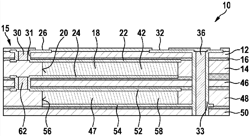
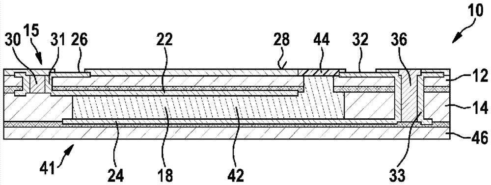
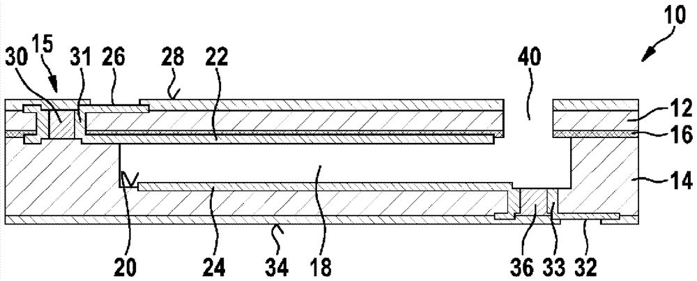
[0040] in figure 1 The first embodiment of the carrier according to the invention shown in is indicated by the reference numeral 10 as a whole. The carrier 10 is designed as a circuit board and has a first base layer 12 and a second base layer 14. The two base layers 12, 14 are designed as thermosetting layers that are passed through by glass fibers, for example glass fibers embedded in epoxy resin. The epoxy resin layer is primarily dedicated to the stability of the circuit board and as a carrier for the circuit 15. The standard thickness of the epoxy core is 50 to 710 microns. Furthermore, the carrier 10 has a pre-cured layer 16 arranged between the first base layer 12 and the second base layer 14. The semi-cured layer 16 is designed as a thermosetting synthetic material base and is dedicated to joining the two base layers 12 and 14. The typical semi-cured thickness is 50 to 180 microns.
[0041] In addition, the carrier 10 has a cavity 18. The cavity 18 is disposed betwee...
PUM
| Property | Measurement | Unit |
|---|---|---|
| diameter | aaaaa | aaaaa |
| thickness | aaaaa | aaaaa |
Abstract
Description
Claims
Application Information
 - R&D
- Intellectual Property
- Life Sciences
- Materials
- Tech Scout
- Unparalleled Data Quality
- Higher Quality Content
- 60% Fewer Hallucinations
Browse by: Latest US Patents, China's latest patents, Technical Efficacy Thesaurus, Application Domain, Technology Topic, Popular Technical Reports.
© 2025 PatSnap. All rights reserved.Legal|Privacy policy|Modern Slavery Act Transparency Statement|Sitemap|About US| Contact US: help@patsnap.com


