A shift register unit, gate driving device and display panel

A shift register and gate technology, applied in static memory, digital memory information, instruments, etc., can solve problems such as signal distortion of shift register units, and achieve the goal of solving signal distortion, reducing leakage current, and reducing the influence of leakage current. Effect

Active Publication Date: 2016-04-06
WUHAN TIANMA MICRO ELECTRONICS CO LTD +1
View PDF5 Cites 2 Cited by
  • Summary
  • Abstract
  • Description
  • Claims
  • Application Information

AI Technical Summary

Problems solved by technology

[0006] The purpose of the present invention is to provide a shift register unit, a gate drive device and a display panel to solve the problem of signal distortion of the shift register unit

Method used


Image

  • A shift register unit, gate driving device and display panel
  • A shift register unit, gate driving device and display panel
  • A shift register unit, gate driving device and display panel

Examples


Embodiment 1

[0034] Embodiment 1, taking each transistor as an example of a PMOS transistor for illustration, is as follows:

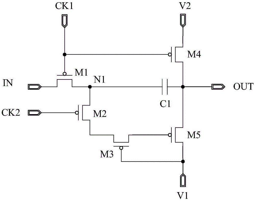
[0035] see figure 2 The first shift register unit provided by the embodiment of the present invention includes: a first transistor M1, the gate of which is electrically connected to the first clock signal terminal CK1, and the first pole thereof is used as the input terminal IN of the shift register unit, and The second pole is electrically connected to the first end of the capacitor C1, and the second end of the capacitor C1 is the output end OUT of the shift register unit;

[0036] The gate of the second transistor M2 is electrically connected to the second clock signal terminal CK2, its first pole is electrically connected to the second pole of the first transistor M1, and its second pole is electrically connected to the first pole of the third transistor M3;

[0037] The gate of the third transistor M3 is electrically connected to the first level signal termi...

Embodiment 2

[0069] Embodiment two, provide such as Figure 5 and Figure 7 The shift register unit shown is the same as that of the first embodiment figure 2 and Figure 4The shift register cell shown has the same element structure, but Figure 5 and Figure 7 Each transistor in the shown shift register unit is an NMOS transistor, the first pole of each NMOS transistor is a source, and the second pole is a drain. The details are as follows:

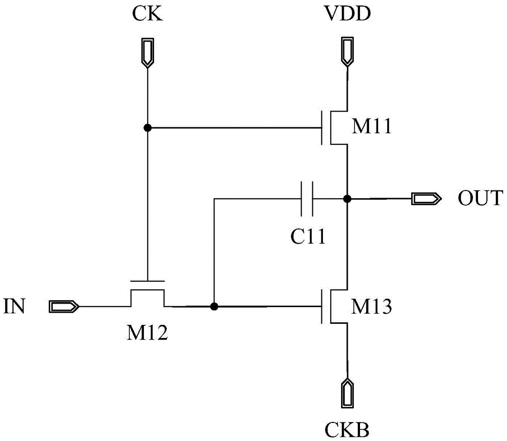
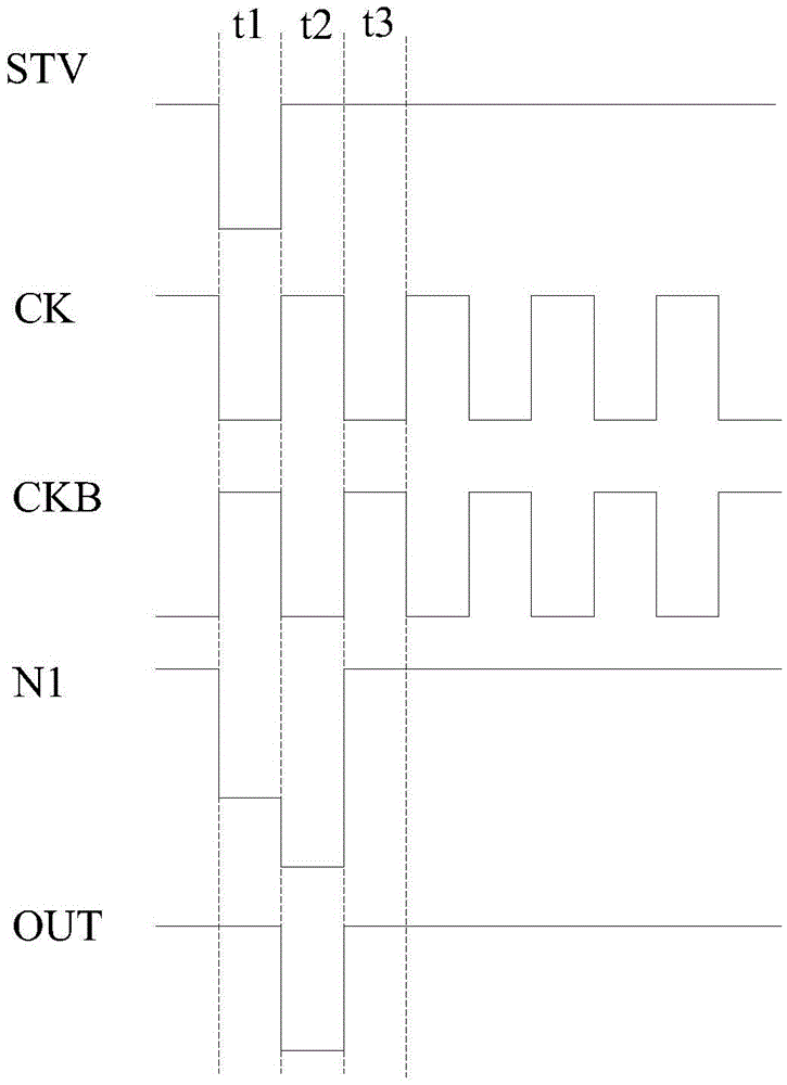
[0070] against Figure 5 and Figure 7 The shift register cell shown, provides Figure 6 The timing diagram of the operation is shown. see Figure 5 , this embodiment provides a schematic structural diagram of the third type of shift register unit. The input terminal IN of the shift register unit is connected to the monostable pulse signal STV, and the monostable pulse signal STV is active at high level; the first clock signal terminal CK1 is connected to the second clock signal CKB, and the second clock signal terminal CK2 The first cloc...

Embodiment 3

[0095] Embodiment three, provide such as Figure 8 and Figure 10 In the shift register unit shown, each transistor is an NMOS transistor. Figure 8 and Figure 10 The shift register unit shown is slightly different from the shift register unit provided in Embodiment 1 or Embodiment 2, and the details are as follows:

[0096] see Figure 8 , the embodiment of the present invention provides a fifth shift register unit, including: the gate of the first transistor M1 is electrically connected to the first clock signal terminal CK1, and its first pole is used as the input terminal IN of the shift register unit, and its second The pole is electrically connected to the first end of the capacitor C1, and the second end of the capacitor C1 is the output end OUT of the shift register unit;

[0097] The gate of the second transistor M2 is electrically connected to the second clock signal terminal CK2, its first pole is electrically connected to the second pole of the first transisto...


PUM


Abstract

The invention discloses a shifting register unit, a grid driving device and a display panel to solve the problem of signal distortion of a shifting register unit. The shifting register unit comprises a first transistor, a second transistor, a third transistor, a fourth transistor and a fifth transistor, wherein the grid of the first transistor is connected with a first clock signal end, the first pole of the first transistor is the input end of the shifting register unit, the second pole of the first transistor is connected with the first end of a capacitor, and the second end of the capacitor is the output end of the shifting register unit; the grid of the second transistor is connected with a second clock signal end, the first pole of the second transistor is connected with the second pole of the first transistor, and the second pole of the second transistor is connected with the first pole of the third transistor; the grid of the third transistor is connected with the first level signal end or the second level signal end, and the second pole of the third transistor is connected with the grid of the fifth transistor; the grid of the fourth transistor is connected with the first clock signal end, the first pole of the fourth transistor is connected with the second level signal end, and the second pole of the fourth transistor is connected with the second end of the capacitor; the second pole of the fifth transistor is connected with the first level signal end, and the first pole of the fifth transistor is connected with the second end of the capacitor.

Description

technical field [0001] The invention relates to the technical field of gate driving of liquid crystal display devices, in particular to a shift register unit, a gate driving device and a display panel. Background technique [0002] In today's era of rapid technological development, liquid crystal displays have been widely used in electronic display products, such as televisions, computers, mobile phones and personal digital assistants. The liquid crystal display includes a data driver (SourceDriver), a gate driver (GateDriver), and a liquid crystal display panel. The liquid crystal display panel has a pixel array, and the gate driving device is used to sequentially turn on the corresponding pixel rows in the pixel array, so as to transmit the pixel data output by the data driver to the pixels, and then display the image to be displayed. [0003] Existing gate drive devices are usually composed of shift register units. Due to the limitations of existing technology, shift reg...

Claims


Application Information

Patent Timeline
Patent Type & Authority Patents(China)
IPC IPC(8): G09G3/36G11C19/28
Inventor 吴桐钱栋
Owner WUHAN TIANMA MICRO ELECTRONICS CO LTD
Why Eureka
Try Eureka