

Wireless charger
A technology of wireless chargers and charging coils, applied in current collectors, electric vehicles, electrical components, etc., can solve the problems of large thickness and inconvenient carrying of wireless chargers, and achieve the effect of reducing the overall thickness and being easy to carry
- Summary
- Abstract
- Description
- Claims
- Application Information
AI Technical Summary
Problems solved by technology
Method used
Image

Examples
Embodiment 1
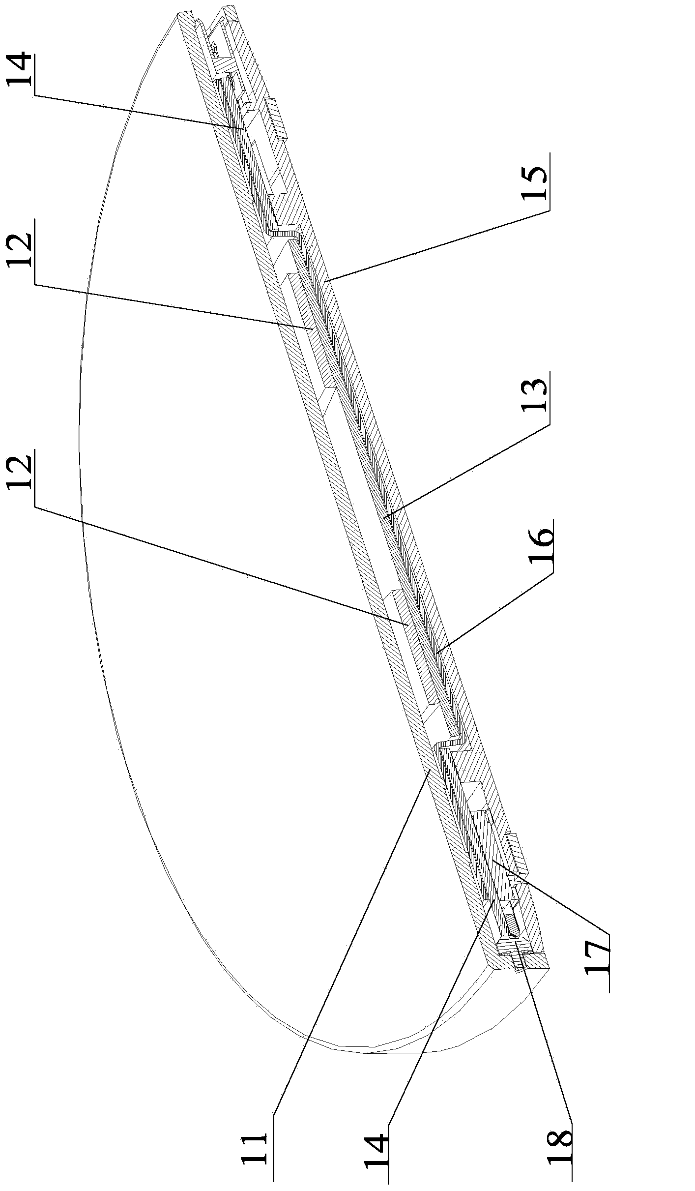
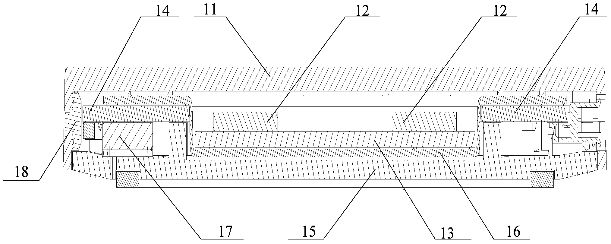
[0025] see figure 1 and figure 2 , figure 1 It is a schematic cross-sectional view of a wireless charger disclosed in the embodiment of this application. figure 2 It is a schematic diagram of planar structure of a wireless charger disclosed in the embodiment of this application.
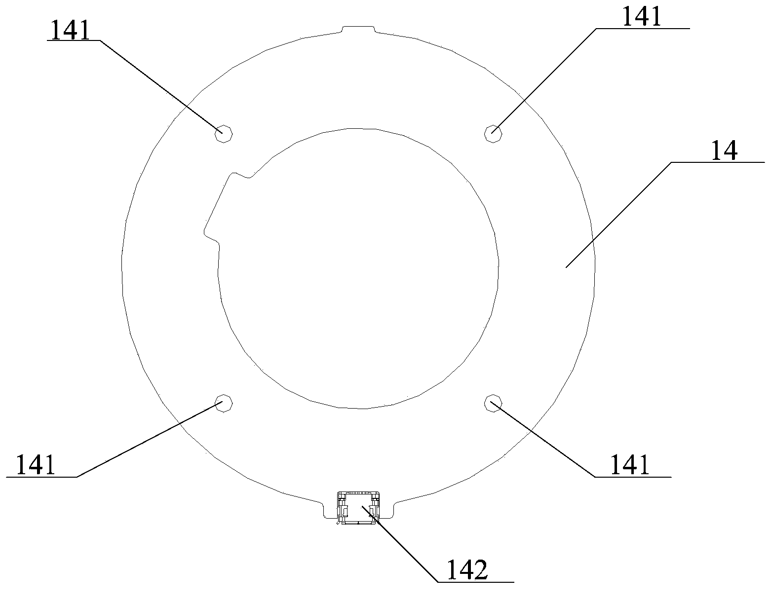
[0026] As shown in the figure, the wireless charger includes an upper cover 11 , a charging coil 12 , a ferrite 13 , a printed circuit board assembly 14 and a lower cover 15 . Wherein, the charging coil 12 is arranged above the ferrite 13 , and the printed circuit board assembly 14 is a hollow structure, and the charging coil 12 and the ferrite 13 are placed in the through holes in the middle. Finally, the upper cover 11 and the lower cover 15 are added together to form a wireless charger.
[0027] Since the printed circuit board assembly 14 is designed as a hollow structure, the charging coil 12 and the ferrite 13 can be placed inside the printed circuit board assembly 14, so that the charging...
Embodiment 2
[0029] Continue to see attached figure 1 And attached figure 2 , the ferrite 13 in the figure is to prevent the magnetic field generated by the charging coil 12 from affecting the printed circuit board assembly 14, but if the power is strong enough, a single ferrite 13 cannot completely shield the electromagnetic field. Therefore, we A metal bracket 16 is further added between the ferrite 13 and the printed circuit board assembly 14, and the metal bracket 16 further isolates the printed circuit board assembly 14 and the ferrite 13, further ensuring that the electromagnetic field of the charging coil 14 will not Affects the printed circuit board assembly 14.
[0030] Of course, the specific structure of the metal bracket 14 can be varied, as long as the above effects can be achieved. Here we give an example of a more preferred solution:
[0031] We set the metal bracket 16 as figure 2 In the shown structure, the metal bracket 16 presents a groove shape as a whole, a part ...
PUM
 Abstract
Description
Claims
Application Information