

Multi-chip packaging structure and manufacturing method thereof
A technology of multi-chip packaging and manufacturing methods, applied in semiconductor/solid-state device manufacturing, electrical components, electric solid-state devices, etc., can solve the problems of increasing the overall thickness of the multi-chip packaging structure, increasing the collapse of wire arcs, etc., and avoiding the collapse of welding wires , the overall thickness reduction, the effect of reducing height and length
- Summary
- Abstract
- Description
- Claims
- Application Information
AI Technical Summary
Problems solved by technology
Method used
Image

Examples
Embodiment Construction
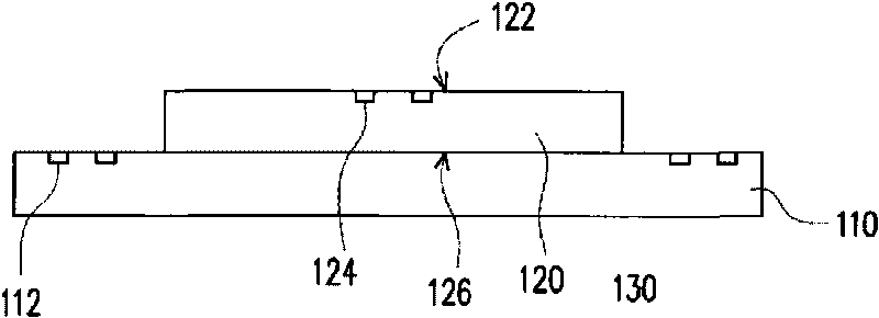
[0060] Figure 1A to Figure 1I It is a schematic cross-sectional view of a manufacturing method of a chip packaging structure according to an embodiment of the present invention, and Figure 2A and Figure 2B for Figure 1B top view. First, please refer to Figure 1A , providing a carrier 110, and disposing a first chip 120 with a first active surface 122, a plurality of first pads 124 on the first active surface 122 and a first back surface 126 on the carrier 110 on. In this embodiment, the carrier 110 is a circuit board, wherein the circuit board can be FR4, FR5, BT, PI circuit substrate, and the material of the lead frame is copper or other suitable conductive materials. From Figure 1A It can be seen that when the carrier 110 is a circuit board, it may have a plurality of third pads 112 .
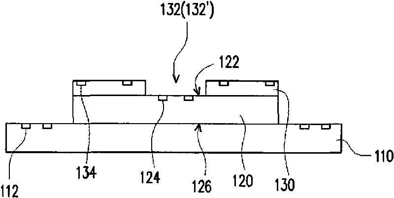
[0061] Next, please refer to Figure 1B , will have an opening 132 (such as Figure 2A as shown) or a notch 132' (such as Figure 2B As shown), the relay circuit substrate 130 ...
PUM
 Abstract
Description
Claims
Application Information