Check patentability & draft patents in minutes with Patsnap Eureka AI!

Input device, display device, and electronic device

A technology of input device and display device, which is applied in the input/output process of data processing, electrical digital data processing, instruments, etc., can solve the problem of reduced noise resistance and achieve the effect of suppressing the reduction of noise resistance

Active Publication Date: 2014-08-13
JAPAN DISPLAY INC
View PDF7 Cites 0 Cited by
  • Summary
  • Abstract
  • Description
  • Claims
  • Application Information

AI Technical Summary

Problems solved by technology

Therefore, there is a possibility that the degree of freedom of the detection capacitance detected on the drive electrodes having such different widths with respect to the upper limit value or the lower limit value of the ADC range becomes smaller, and the noise resistance of the detection capacitance decreases.

Method used


Image

  • Input device, display device, and electronic device
  • Input device, display device, and electronic device
  • Input device, display device, and electronic device

Examples


Embodiment approach 1

[0071]

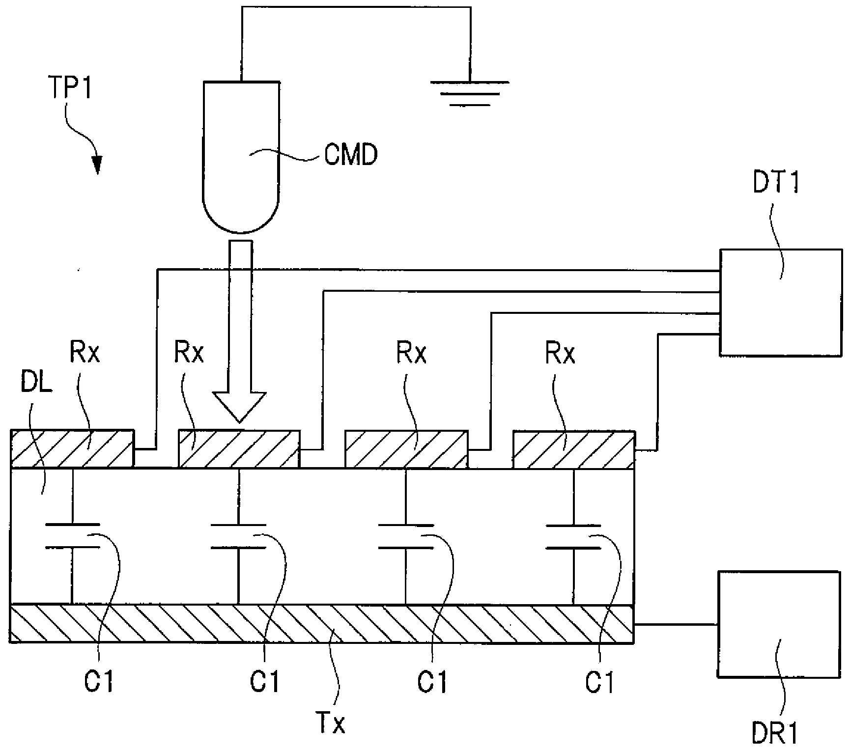
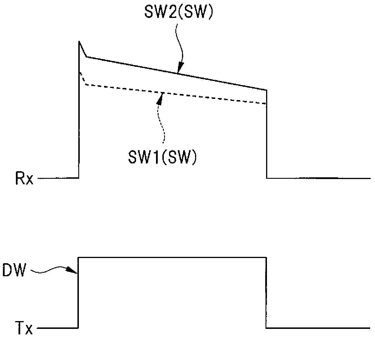
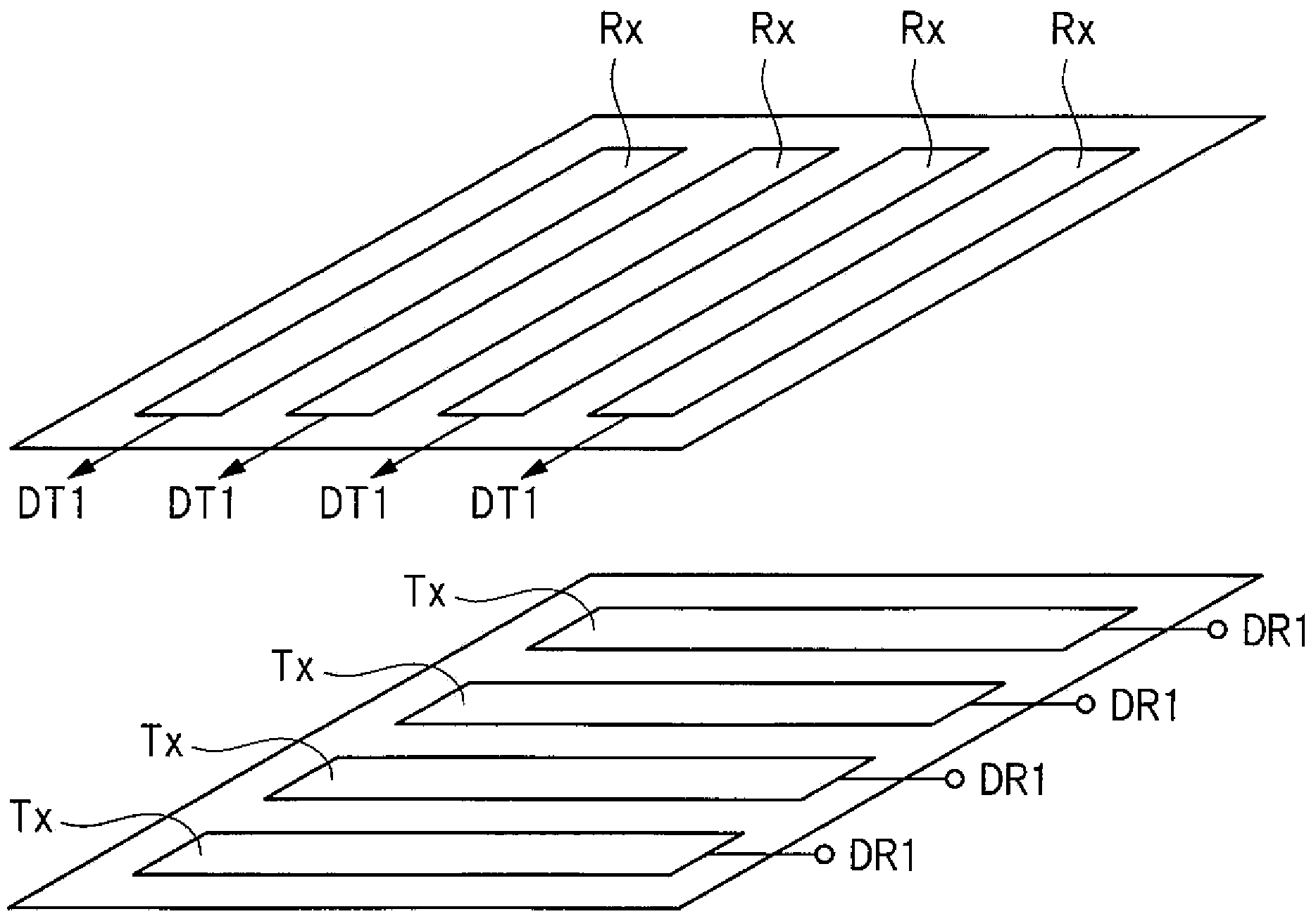
[0072] First, the basic operating principle of the input device of the so-called capacitive touch panel or touch sensor will be described. figure 1 It is an explanatory diagram showing a schematic configuration of a capacitive touch panel. also, figure 2 yes show right figure 1 An explanatory diagram showing an example of the relationship between the drive waveform applied to the touch panel and the signal waveform output from the touch panel. and, image 3 is modeled figure 1 An explanatory diagram of an example of the arrangement of the drive electrodes and the detection electrodes shown.

[0073] Capacitive touch panel TP1 as an input device has a plurality of drive electrodes Tx and a plurality of detection electrodes Rx. The drive electrode Tx and the detection electrode Rx are arranged facing each other with the dielectric layer DL interposed therebetween, and the capacitive element C1 is formed by the drive electrode Tx, the dielectric layer DL, and the...

Embodiment approach 2

[0204] In Embodiment 1, in order to adjust the electrostatic capacitance between the driving electrode and the detection electrode having a width smaller than that of other driving electrodes, the enlarged portion for expanding the area of ​​the electrode is provided outside the display area in plan view. On the other hand, in Embodiment 2, in order to adjust the capacitance between the driving electrode and the detecting electrode having a width smaller than that of other driving electrodes, the expansion part that expands the area of ​​the detecting electrode is provided at the area having the small width in plan view. on the driving electrodes.

[0205] Parts other than the touch panel TP2 in the display device according to the second embodiment are the same as parts other than the touch panel TP1 in the display device according to the first embodiment, and thus description thereof will be omitted.

[0206]

[0207] Figure 16 It is a plan view schematically showing the ...

Embodiment approach 3

[0276] In Embodiment 2, in plan view, adjustment is made such that the area of ​​the portion of the detection electrode that overlaps the drive electrode having a width smaller than that of the other drive electrodes is larger than the area of ​​the portion of the detection electrode that overlaps with the other electrodes. In this regard, in the third embodiment, in the plan view, adjustment is made such that the area of ​​the overlapping portion of the detection electrode with the driving electrode having a width larger than that of other driving electrodes is smaller than the area of ​​the overlapping portion of the detection electrode with other driving electrodes.

[0277] Parts other than the touch panel TP3 in the display device according to the third embodiment are the same as parts other than the touch panel TP1 in the display device according to the first embodiment, and description thereof will be omitted.

[0278]

[0279] Figure 23 It is a plan view schematical...


PUM


Abstract

A noise immunity of a detected capacitance is prevented or inhibited from lowering on a driving electrode different in width from the other driving electrodes, provided in an input device. A touch panel serving as an input device has a plurality of driving electrodes extending in an X-axis direction and arranged in a Y-axis direction intersecting with the X-axis direction, and a driving electrode arranged outside one side of an arrangement of the driving electrodes and extending in the X-axis direction. Further, the touch panel TP1 has a plurality of detecting electrodes extending in the Y-axis direction and arranged in the X-axis direction. The width of the driving electrode is smaller than the widths of the driving electrodes and the detecting electrode includes an expanding portion for expanding the area of the detecting electrode on the side opposite to the plurality of driving electrodes via the driving electrode.

Description

technical field [0001] The present invention relates to an input device, a display device, and electronic equipment, and more particularly, to a capacitive input device, and a display device and electronic equipment including such an input device. Background technique [0002] In recent years, an input device called a touch panel or a touch sensor is installed on the display surface side of a display device, and an input device such as a finger or a stylus is brought into contact with the touch panel to perform an input operation by detecting and outputting an input position. Since a display device having such a touch panel does not require an input device such as a keyboard, a mouse, or a keypad, it is widely used in mobile information terminals such as mobile phones and the like in addition to computers. [0003] One detection method for detecting a contact position of a finger or the like on the touch panel is a capacitive method. In a capacitive touch panel, a pair of e...

Claims


Application Information

Patent Timeline
Patent Type & Authority Applications(China)
IPC IPC(8): G06F3/044
CPCG06F3/044G06F3/0445G06F3/0446G06F3/04166G06F3/0448G06F3/0412G06F3/0416
Inventor 寺西康幸铃木崇章安住康平
Owner JAPAN DISPLAY INC
Features
  • R&D
  • Intellectual Property
  • Life Sciences
  • Materials
  • Tech Scout
  • Unparalleled Data Quality
  • Higher Quality Content
  • 60% Fewer Hallucinations
Learn More