Silicon capacitor vacuum sensor based on micro electro mechanical system (MEMS) technology

A technology of vacuum sensor and micro-electro-mechanical system, applied in vacuum gauges, instruments, measuring devices, etc., can solve problems such as film rupture and adhesion failure, and achieve the effects of reducing nonlinearity, high-precision measurement, and avoiding adhesion failure

Inactive Publication Date: 2014-08-20
江苏森博传感技术有限公司
View PDF13 Cites 16 Cited by
  • Summary
  • Abstract
  • Description
  • Claims
  • Application Information

AI Technical Summary

Problems solved by technology

[0009] The present invention aims at the deficiencies of the above-mentioned prior art, and provides a micro-capacitance thin-film sensor that can effectively measure high vacuum, cover a large range of vacuum, and have a simple manufacturing process, and solve the problem of sensitive film rupture, adhesion failure, and outgassing of glass materials in the prior art. Problems of Silicon Capacitive Vacuum Sensors Based on MEMS Technology

Method used


Image

  • Silicon capacitor vacuum sensor based on micro electro mechanical system (MEMS) technology
  • Silicon capacitor vacuum sensor based on micro electro mechanical system (MEMS) technology
  • Silicon capacitor vacuum sensor based on micro electro mechanical system (MEMS) technology

Examples


Embodiment 1

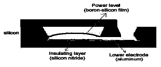
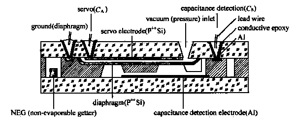
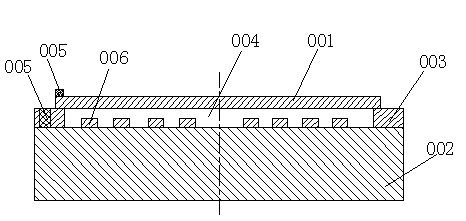
[0035] Embodiment 1: A silicon capacitive vacuum sensor based on MEMS technology, including an upper plate 001, a lower plate 002, an intermediate insulating layer 003, a vacuum chamber 004, and electric lead welding on the upper and lower plates (001, 002) The disc 005, the upper plate 001 is a silicon sensitive film, the vacuum chamber 004 is a sealed cavity formed between the upper plate 001, the intermediate insulating layer 003 and the lower plate 002, and an array of insulating support columns 006 is designed in the vacuum chamber 004. There is a gap between the top surface of the insulating support column 006 and the upper plate 001, the thickness of the silicon sensitive film is 5um, the intermediate insulating layer 003 is silicon dioxide, the thickness of the intermediate insulating layer 003 is 2um, and the insulating support column 006 The insulating support pillars 006 in the array are evenly distributed, the shape of the cross-section of the insulating support pil...

Embodiment 2

[0036] Embodiment 2: Referring to Embodiment 1, the thickness of the silicon sensitive film is 10um, the thickness of the intermediate insulating layer 003 is 5um, and each insulating support pillar in the array of insulating support pillars 006 is non-uniformly distributed, and the shape of the cross section of the insulating support pillar 006 is Square, different sizes and dimensions, the cross-sectional area of ​​the insulating support column 006 is 1um 2 -1mm 2 The distance between the insulating support pillars 006 is the same, and the distance is 500 microns.

Embodiment 3

[0037] Embodiment 3, with reference to Embodiment 1, the vacuum chamber 004 is a sealed cavity formed between the upper plate 001 and the intermediate insulating layer 003, the intermediate insulating layer 003 is a composite of a silicon dioxide layer and a silicon nitride layer, and the intermediate insulating layer The thickness of the silicon sensitive film is 3um, and the thickness of the silicon sensitive film is 0.5um. The insulating support pillars in the array of insulating support pillars 006 are non-uniformly distributed. The cross-sectional area is 100um 2 , the spacing between the insulating support pillars 006 is different, and the spacing is between 0-800 microns.


PUM

PropertyMeasurementUnit
breaking strengthaaaaaaaaaa

Abstract

A silicon capacitor vacuum sensor based on micro electro mechanical system (MEMS) technology relates to the field of micro electro mechanical system (MEMS) sensor and vacuum sensor manufacture. The silicon capacitor vacuum sensor comprises an upper polar plate, a lower polar plate, a middle insulating layer, a vacuum cavity and electrical lead bonding pads on the upper polar plate and the lower polar plate. The vacuum cavity is a sealed cavity formed by the upper polar plate and the middle insulating layer, or the upper polar plate, the middle insulating layer and the lower polar plate. The vacuum cavity is internally provided with an insulation support column array. A gap is left between each top surface of each insulation support column and the upper polar plate. The silicon capacitor vacuum sensor can effectively measure high vacuum degree; the vacuum degree coverage range is large; manufacture process is simple; and the problems of sensitive film breaking, adherence failure and the used glass material outgassing and the like in a miniature capacitor film sensor in the prior art are effectively solved.

Description

technical field [0001] The invention relates to a micro-electro-mechanical system (MEMS) sensor, in particular to a silicon capacitive vacuum sensor based on the micro-electro-mechanical system technology. Background technique [0002] The miniature capacitive film vacuum sensors disclosed in the prior art include: (1) Xiamen University has studied "capacitive miniature vacuum sensors based on MEMS technology", such as figure 1 As shown, the capacitive vacuum sensor has two cavities, the upper cavity is a vacuum cavity, and the lower cavity is formed by bonding, and the cavity is not sealed. The vacuum sensor adopts a glass-silicon-glass sandwich structure, which is composed of a glass substrate, a lower electrode, an insulating layer, a silicon diaphragm (upper electrode), and glass for upper sealing. The lower electrode is sputtered on the glass substrate. , an insulating layer is grown on the electrode, and the silicon film is formed by double-sided photolithography, dif...

Claims


Application Information

Patent Timeline
Patent Type & Authority Applications(China)
IPC IPC(8): G01L21/00
Inventor 吴亚明刘京孙艳美姚朝辉徐永康
Owner 江苏森博传感技术有限公司
Why Eureka
Try Eureka