Optical imaging lens and electronic device with optical imaging lens

A technology of optical imaging lens and imaging surface, which is applied in the field of optical lens, can solve the problems that are not conducive to thin design, achieve the effect of light, thin and small structure design, meet consumer demand, and good optical performance

Active Publication Date: 2014-08-27
GENIUS ELECTRONICS OPTICAL XIAMEN
View PDF11 Cites 7 Cited by
  • Summary
  • Abstract
  • Description
  • Claims
  • Application Information

AI Technical Summary

Problems solved by technology

Among them, the lens length of US Patent Publication No. 20110316969 is more than 14mm, which is not conducive to the thin design of portable electronic products such as mobile phones and digital cameras.

Method used


Image

  • Optical imaging lens and electronic device with optical imaging lens
  • Optical imaging lens and electronic device with optical imaging lens
  • Optical imaging lens and electronic device with optical imaging lens

Examples


Embodiment Construction

[0117] Before the present invention is described in detail, it should be noted that in the following description, similar components are denoted by the same numerals.

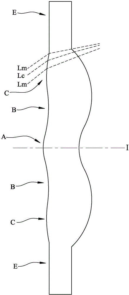
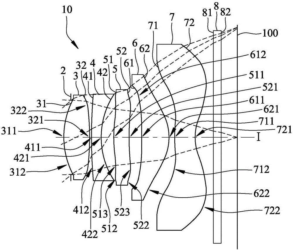
[0118] The expression "a lens has positive refractive power (or negative refractive power)" in this specification means that the lens has positive refractive power (or negative refractive power) in the vicinity of the optical axis. "The object side (or image side) of a lens has a convex surface (or concave surface) located in a certain area" means that the area is closer to the direction parallel to the optical axis than the radially outer area of ​​the area. For "convex" (or "concave"), the figure 1 For example, where I is the optical axis and the lens is radially symmetrical to each other with the optical axis I as the axis of symmetry, the object side of the lens has a convex surface in the A region, a concave surface in the B region, and a convex surface in the C region , the reason is that compared with t...


PUM


Abstract

The invention relates to an optical imaging lens and an electronic device with the optical imaging lens. The optical imaging lens sequentially comprises five lens bodies from the object side to the image side. The image side face of the first lens body is provided with a convex face part located in the area near the circumference; the object side face of the second lens body is provided with a convex face part located in the area near the circumference, and the image side face of the second lens body is provided with a concave face part located in the area near the optical axis; the image side face of the third lens body is provided with a concave face part located in the area near the circumference; the object side face of the fourth lens body is provided with a concave face part located in the area near the optical axis; the image side face of the fifth lens body is provided with a concave face part located in the area near the optical axis, and the condition that ALT/G34<=7.7 is met. The camera device comprises an enclosure and an image module and further comprises the optical imaging lens, a lens cone, a module back seat unit and an image sensor. Thus, the lens length can be reduced, and good imaging quality can be kept.

Description

technical field [0001] The invention relates to an optical lens, in particular to an optical imaging lens and an electronic device using the optical imaging lens. Background technique [0002] In recent years, the popularization of portable electronic products such as mobile phones and digital cameras has led to the vigorous development of imaging module related technologies. The imaging module mainly includes components such as optical imaging lens, module holder unit and sensor. The thin and light trend of digital cameras also makes the miniaturization of image modules more and more demanding. For the technological progress and size reduction of CMOS), the length of the optical imaging lens loaded in the image module also needs to be shortened accordingly. performance. [0003] U.S. Patent Publication Nos. 20110316969, 20100254029, 20130107376, 20130057967, U.S. Patent Publication Nos. 8,345,323, 7,911,712, and Japanese Patent Publication No. 2008-281760 all disclose an ...

Claims


Application Information

Patent Timeline
Patent Type & Authority Applications(China)
IPC IPC(8): G02B13/18G02B7/02
CPCG02B13/0045G02B9/60G02B13/0015
Inventor 陈思翰陈锋张仲志
Owner GENIUS ELECTRONICS OPTICAL XIAMEN
Why Eureka
Try Eureka