
Touch display panel and touch display device

A touch display panel and substrate technology, which is applied in optics, instruments, electrical digital data processing, etc., can solve the problems of low production efficiency, high cost, cumbersome process, etc., and achieve the goal of improving production efficiency, reducing cost, and avoiding mutual influence Effect

Active Publication Date: 2017-02-15
KUSN INFOVISION OPTOELECTRONICS
View PDF5 Cites 0 Cited by
  • Summary
  • Abstract
  • Description
  • Claims
  • Application Information

AI Technical Summary

Problems solved by technology

[0005] It can be seen from the structure of the main capacitive touch screens mentioned above that the existing capacitive touch technology needs to combine the touch sensor and / or cover lens with the liquid crystal display panel through a full lamination process. However, the process is cumbersome, the cost is high, and the production efficiency is low

Method used


Image

  • Touch display panel and touch display device
  • Touch display panel and touch display device
  • Touch display panel and touch display device

Examples


Embodiment Construction

[0022] In order to further explain the technical means and effects of the present invention to achieve the intended purpose of the invention, the specific implementation, structure, features and effects of the present invention will be described in detail below in conjunction with the accompanying drawings and preferred embodiments.

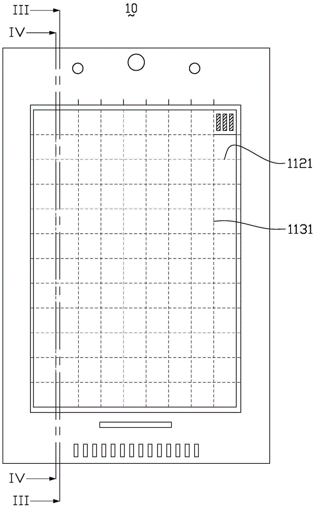
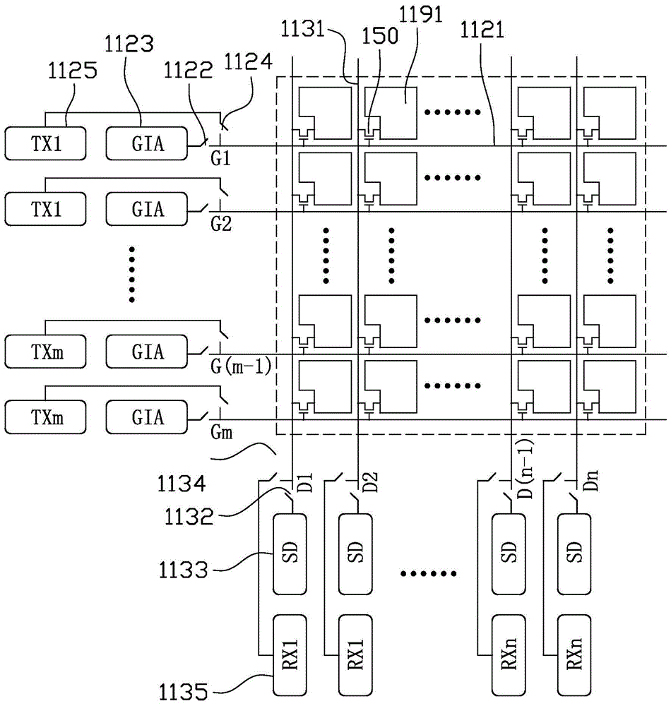
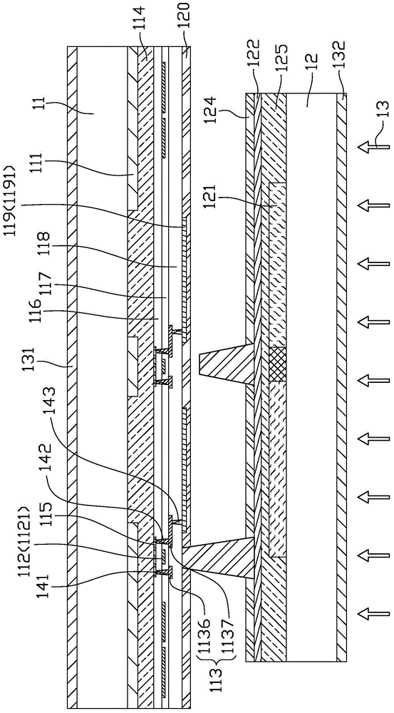
[0023] figure 1 is a schematic plan view of the touch display panel in an embodiment of the present invention, figure 2 is a schematic diagram of the circuit structure of the first substrate in the embodiment of the present invention, such as figure 1 and figure 2 As shown, the touch display panel 10 of the embodiment of the present invention includes gate lines 1121 (respectively G1, G2, . D1, D2, ..., D(n-1), Dn, n is a positive integer), the gate line 1121 and the data line 1131 are intersected to form a plurality of pixel units arranged in a matrix, each pixel unit is provided with a pixel The electrode 1191 is connected to a thin-film t...


PUM


Abstract

A touch display panel comprises a first substrate and a second substrate opposite to the first substrate, wherein the first substrate is located above the second substrate to enable he first substrate to be located on one side close to a user, grid lines and data lines are formed on one side of the first substrate close to the second substrate and intersected to form multiple pixel units arranged in a matrix mode, a pixel electrode and an oxide thin-film transistor are arranged in each pixel unit, the pixel electrodes are connected with the grid lines and data lines through the oxide thin-film transistors, at least one portion of the grid lines concurrently serves as one of touch driving lines and touch sensing lines, at least one portion of the data lines concurrently serves as the other one of the touch driving lines and the touch sensing line, the grid lines and the data lines receive image scanning signals and data signals at an image display stage for image display and receives touch driving signals and output touch sensing signals at a touch detection stage for touch detection.

Description

technical field [0001] The present invention relates to the field of display technology, in particular to a touch display panel and a touch display device. Background technique [0002] With the development of the information age and the acceleration of the pace of life, touch technology has gradually replaced the traditional mouse and keyboard due to its humanized design and simple and fast input, and is widely used in various electronic products. Such as: mobile phones, computers, personal digital assistants, etc. According to different sensing principles, touch panels are divided into: resistive, capacitive, optical, acoustic, and electromagnetic. Since the capacitive touch display panel has the advantages of fast response, high sensitivity, good reliability and high durability, the capacitive touch display panel has been widely used at present. [0003] The capacitive touch screen mainly includes a protective glass (Cover Lens) and a touch sensor (Touch Sensor). There...

Claims


Application Information

Patent Timeline
Patent Type & Authority Patents(China)
IPC IPC(8): G02F1/1333G02F1/1368G06F3/041
Inventor 戴文君
Owner KUSN INFOVISION OPTOELECTRONICS
Learn More