Radio frequency and base band integrated circuit

An integrated circuit and baseband technology, applied in circuits, electrical components, electrical solid state devices, etc., can solve problems such as high testing costs, achieve the effects of reducing costs and risks, shortening the research and development cycle, and accelerating market promotion

Inactive Publication Date: 2014-09-17
TECHTOTOP MICROELECTRONICS
View PDF1 Cites 6 Cited by
  • Summary
  • Abstract
  • Description
  • Claims
  • Application Information

AI Technical Summary

Problems solved by technology

[0008] Based on the above situation, the purpose of the present invention is to provide a radio frequency baseband integrated circuit, which can increase the testability of the radio frequency chip, increase the test coverage of the radio frequency and the internal interconnection of the ba

Method used


Image

  • Radio frequency and base band integrated circuit
  • Radio frequency and base band integrated circuit
  • Radio frequency and base band integrated circuit

Examples


Embodiment Construction

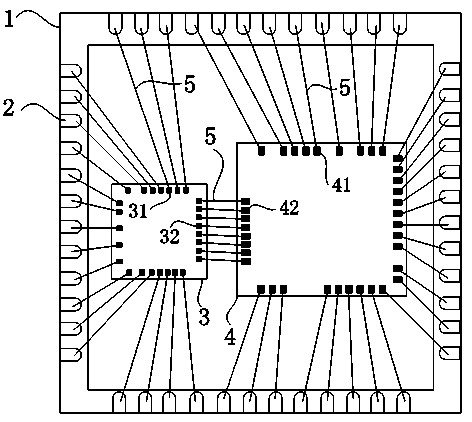
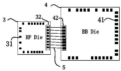
[0017] The radio frequency chip and baseband chip of the SiP device in the prior art generally adopt the stacking method of bare chips. Engineering practice shows that the stacking method of the radio frequency chip and the baseband chip is extremely vulnerable to the interference of the high-speed digital signal inside the baseband chip and reduces the performance of the radio frequency itself. . In addition, since the size of the radio frequency chip is usually smaller than the baseband chip, the stacking method is also likely to make the input signal bonding of the radio frequency chip longer, introduce larger package parasitic parameters, and eventually lead to a decrease in the overall performance of the navigation chip.

[0018] The selection of conventional BGA packaging in SiP devices is also a commonly used technology, but it will also bring the following two adverse effects: First, the BGA package has a substrate, and the packaging manufacturing process is relatively ...


PUM


Abstract

The invention provides a radio frequency and base band integrated circuit which comprises a sip chip (1) and external pins (2). The sip chip comprises a radio frequency chip (3) and a base band chip (4), and bonding pads (31) of the radio frequency chip (3) are connected with the external pins (2) through binding wires (5). Bonding pads (41) of the base band chip (4) are connected with the external pins (2) through binding wires (5). Bonding pads (32) of the radio frequency chip (3) are electrically connected with bonding pads (42) of the base band chip (4) through binding wires (5). The problem that an existing navigation chip is large in size can be effectively solved, besides, the research and development cycle of the product can be shortened, cost and risks are reduced, and market access of the product is accelerated.

Description

technical field [0001] The invention relates to the field of hardware, in particular to a radio frequency baseband integrated circuit. Background technique [0002] With the rapid promotion of the Beidou satellite navigation and positioning system, terminal applications on the market tend to be miniaturized and differentiated. This also requires that the size of the navigation chip must be reduced to meet various form requirements. [0003] In response to the above situation, there are currently some solutions, such as using a lower process to make the size of the navigation baseband chip smaller, using the Embedded RF (Embedded Radio Frequency, embedded radio frequency circuit) solution to make the radio frequency and the baseband into a bare chip , Using system-in-package technology to make RF chips and baseband chips into BGA (Ball Grid Array, spherical contact array, one of the surface mount packages) packaged SiP chips (System in Package, system-in-package), etc. But ...

Claims


Application Information

Patent Timeline
IPC IPC(8): H01L25/065
CPCH01L2224/05553H01L2224/48137H01L2224/49171H01L2224/023H01L2924/0001
Inventor 郭金才
Owner TECHTOTOP MICROELECTRONICS
Why Eureka
Try Eureka