Modulation circuit of digital transmitter, digital transmitter and signal modulation method

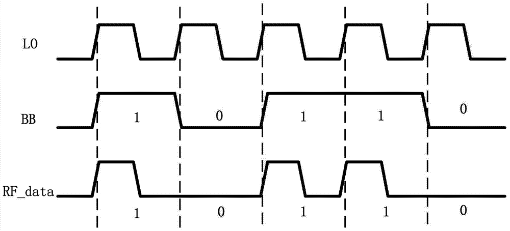
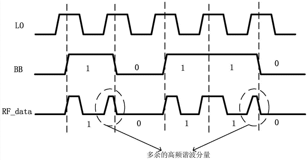
A modulation circuit and digital modulator technology, applied in the field of digital transmitter and signal modulation, modulation circuit of digital transmitter, can solve the problem of difficult digital baseband signal BB edge alignment, introduction of digital baseband signal BB phase noise, excess radio frequency signal Problems such as high frequency harmonic components

Active Publication Date: 2017-07-14
HUAWEI TECH CO LTD
View PDF3 Cites 0 Cited by
  • Summary
  • Abstract
  • Description
  • Claims
  • Application Information

AI Technical Summary

Problems solved by technology

[0004] In fact, when the frequency of the local oscillator signal LO and the data rate of the digital baseband signal BB are as high as GHz (G samples / s), coupled with the presence of voltage, temperature and process deviations, it is difficult to make the digital baseband signal BB and local oscillator signal LO edge aligned
like figure 2 As shown, the logical AND operation is performed when the edges of the digital baseband signal BB and the local oscillator signal LO are not aligned, which will cause redundant high-frequency harmonic components in the modulated radio frequency signal RF_data, and introduce harmonic components from the digital baseband signal BB phase noise

Method used


Image

  • Modulation circuit of digital transmitter, digital transmitter and signal modulation method
  • Modulation circuit of digital transmitter, digital transmitter and signal modulation method
  • Modulation circuit of digital transmitter, digital transmitter and signal modulation method

Examples


Embodiment Construction

[0069] In order to make the object, technical solution and advantages of the present invention clearer, the present invention will be further described in detail below in conjunction with the accompanying drawings. Obviously, the described embodiments are only some embodiments of the present invention, rather than all embodiments . Based on the embodiments of the present invention, all other embodiments obtained by persons of ordinary skill in the art without making creative efforts belong to the protection scope of the present invention.

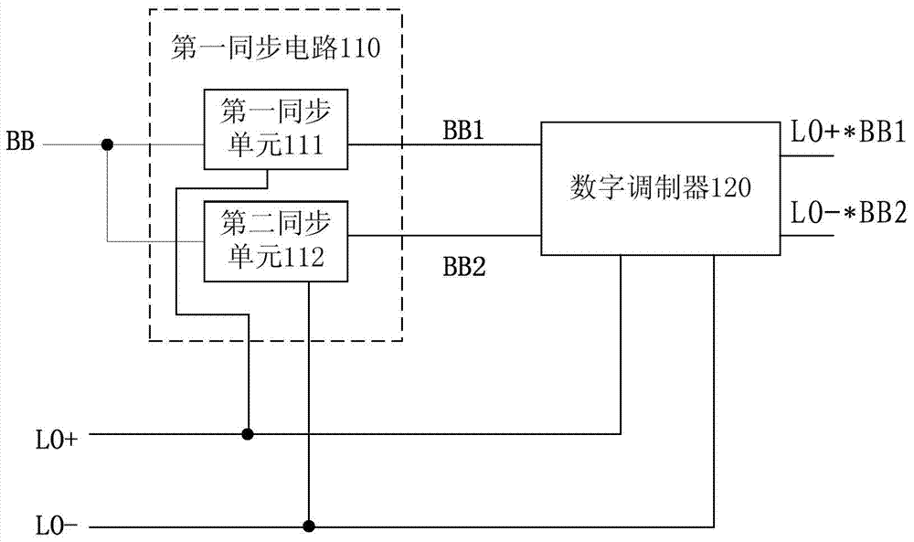
[0070] Below to image 3 As an example, a modulation circuit of a digital transmitter provided in Embodiment 1 of the present invention is described in detail. image 3 It is a schematic structural diagram of a modulation circuit of a digital transmitter provided by Embodiment 1 of the present invention. Such as image 3 As shown, the modulation circuit of the digital transmitter provided in this embodiment includes: a first synchronizat...


PUM


Abstract

The invention relates to a modulation circuit of a digital transmitter, a digital transmitter and a signal modulation method. The modulation circuit includes: a first synchronous circuit and a digital modulator; wherein, the first synchronous circuit includes a first synchronous unit and a second synchronous unit, which respectively phase-delay the first local oscillator signal or the second local oscillator signal Obtain the corresponding delay signal, and use the delay signal to adjust the phase of the digital baseband signal to generate the first adjustment signal and the second adjustment signal, so that the rising edge and falling edge of the first adjustment signal respectively fall on the first phase In the low-level interval of the oscillator signal; and the rising edge and falling edge of the second adjustment signal respectively fall in the low-level interval of the second local oscillator signal; the digital modulator uses the first local oscillator signal to perform the first adjustment signal modulating, generating a first radio frequency signal, and modulating the second adjustment signal with the second local oscillator signal to generate a second radio frequency signal.

Description

technical field [0001] The invention relates to the technical field of wireless communication, in particular to a modulation circuit of a digital transmitter, a digital transmitter and a signal modulation method. Background technique [0002] Currently, mainstream digital transmitters are divided into digital quadrature transmitters (Digital Cartesian Transmitter, DCT) and digital polar transmitters (Digital Polar Transmitter, DPT). Digital modulator for radio frequency signals. [0003] Existing digital modulators usually modulate a digital baseband signal (Baseband, BB) with a local oscillator signal LO through a logic gate (AND gate). Such as figure 1 As shown, to ensure that the modulated radio frequency signal RF_data achieves an ideal waveform, it is necessary to control the phase of the digital baseband signal BB and the local oscillator signal (local frequency, LO) well before the digital baseband signal BB and the local oscillator signal LO enter the logic gate. ...

Claims


Application Information

Patent Timeline
Patent Type & Authority Patents(China)
IPC IPC(8): H04L27/36H03L7/10
CPCH04L27/2092H04L27/365H04B1/0475H04L7/0331H04L7/0337H04L27/364H03L7/00
Inventor 汪吴峰易岷朱年勇莫秉轩
Owner HUAWEI TECH CO LTD
Why Eureka
Try Eureka