Light source module
A light source module and light-incident surface technology, applied in optics, nonlinear optics, instruments, etc., can solve the problems of occupying circuit board layout space, unfavorable narrow frame design of liquid crystal display, etc., and achieve the goal of reducing size and facilitating narrow frame design Effect
- Summary
- Abstract
- Description
- Claims
- Application Information
AI Technical Summary
Problems solved by technology
Method used
Image

Examples
no. 1 example
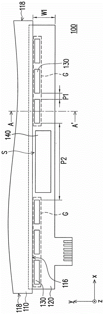
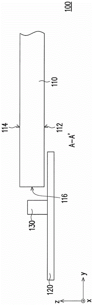
[0066] figure 1 is a schematic diagram of a light source module according to the first embodiment of the present application, and figure 2 for along figure 1 A cross-sectional view of line A-A'. Please refer to figure 1 and figure 2For example, the light source module 100 of this embodiment can be used to provide a backlight for a liquid crystal display, and the light source module 100 includes a light guide plate 110 , a circuit board 120 , a plurality of light emitting elements 130 and a first electronic element 140 . The light guide plate 110 has a bottom surface 112 , a top surface 114 , a light incident surface 116 between the bottom surface 112 and the top surface 114 , and a side surface 118 , wherein the side surface 118 is located between the bottom surface 112 and the top surface 114 and connected to the light incident surface 116 . The circuit board 120 is adjacent to the light incident surface 116 . The plurality of light emitting elements 130 and the first ...
no. 2 example
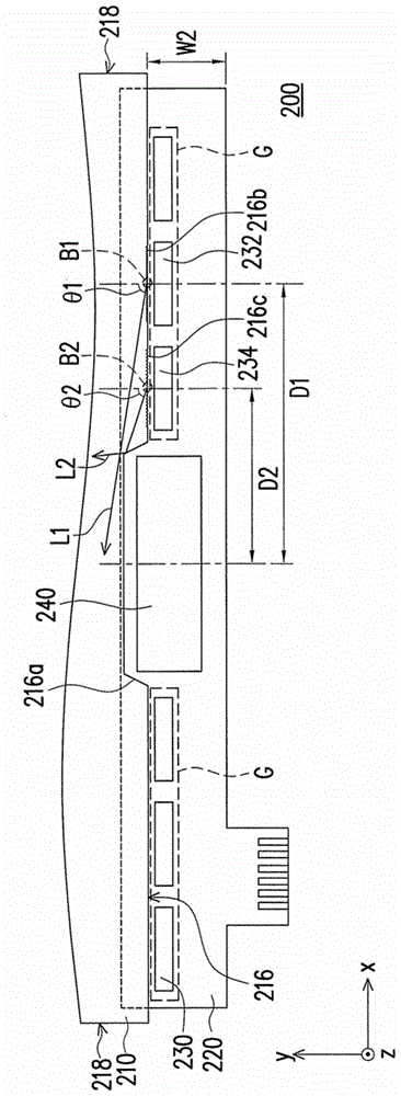
[0071] image 3 is a schematic diagram of a light source module 200 according to the second embodiment of the present application. Please refer to image 3 , the light source module 200 of this embodiment has a similar structure and function to the light source module 100 of the first embodiment, the main difference between them is that: the light incident surface 216 of this embodiment has a first concave portion 216a, and at least a part The first electronic component 240 is located in the first concave portion 216a.
[0072] In this embodiment, the size of the first recessed portion 216 a can be adjusted according to requirements, so as to accommodate at least a part or all of the first electronic components 240 . In other words, by disposing at least a part of the first electronic component 240 in the first recessed portion 216a, the width W2 of the circuit board 120 in the Y direction can be further shortened.
[0073] Considering that the position of the light-emittin...
no. 3 example
[0077] Figure 5 is a schematic diagram of a light source module according to the third embodiment of the present application. In the present application, besides being divided into multiple groups, the light emitting elements can also be arranged on the circuit board collectively, leaving space on both sides of the circuit board for placement of electronic components. Please refer to Figure 5 , in this embodiment, there is a second pitch P2 between the first side 318a and the adjacent light emitting element 330, and there is a third pitch P3 between the second side 318b and the adjacent light emitting element 330, wherein the second pitch P2 and the third pitch P3 are respectively greater than the first pitch P1. By concentrating and arranging the light emitting elements 330 on the circuit board 320 , the space S on both sides of the circuit board 320 is vacated. In this way, the first electronic component 340 and the second electronic component 350 can be arranged in the...
PUM
 Abstract
Description
Claims
Application Information
 - R&D
- Intellectual Property
- Life Sciences
- Materials
- Tech Scout
- Unparalleled Data Quality
- Higher Quality Content
- 60% Fewer Hallucinations
Browse by: Latest US Patents, China's latest patents, Technical Efficacy Thesaurus, Application Domain, Technology Topic, Popular Technical Reports.
© 2025 PatSnap. All rights reserved.Legal|Privacy policy|Modern Slavery Act Transparency Statement|Sitemap|About US| Contact US: help@patsnap.com