Single connecting rod column and circular ring cylinder based large absolute forbidden band square lattice photonic crystal

A photonic crystal, square lattice technology, applied in the field of wide absolute band gap two-dimensional photonic crystal, can solve the problem of small absolute band gap, and achieve the effect of easy connection and coupling, great convenience and flexibility, and cost reduction

Inactive Publication Date: 2014-10-15
SHENZHEN UNIV
View PDF3 Cites 5 Cited by
  • Summary
  • Abstract
  • Description
  • Claims
  • Application Information

AI Technical Summary

Problems solved by technology

[0005] Traditionally, in order to obtain a large relative forbidden band, non-square lattice structures such as triangular lattice and hexagonal lattice need to be used. However, in the photonic crystal integrated optical path, the use of square lattice structure can make the optical path simple and easy to improve the optical path. Integration, while the absolute band gap of the traditional square lattice photonic crystal is very small, so the square lattice photonic crystal with a large absolute band gap has become the goal that people have been pursuing

Method used


Image

  • Single connecting rod column and circular ring cylinder based large absolute forbidden band square lattice photonic crystal
  • Single connecting rod column and circular ring cylinder based large absolute forbidden band square lattice photonic crystal
  • Single connecting rod column and circular ring cylinder based large absolute forbidden band square lattice photonic crystal

Examples


Embodiment 1

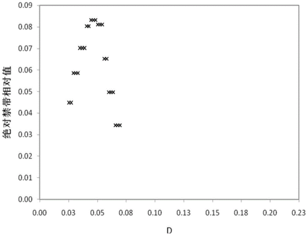
[0040] Embodiment 1. The high refractive index medium adopts silicon, the low refractive index medium is air, the lattice constant a=0.325 of the square lattice photonic crystal, the flat medium column width D=0.048a=0.0156 micron, the ring column outer diameter R= 0.27a=0.08775 microns, the inner diameter of the circular column is 0.061776 microns, the absolute band gap range of the obtained photonic crystal is (0.595718~0.539975), and the relative value of the absolute band gap is 9.8177%.

Embodiment 2

[0041] Embodiment 2. The high refractive index medium adopts silicon, the low refractive index medium is air, the lattice constant a=0.45 of the square lattice photonic crystal, the flat medium column width D=0.048a=0.0216 micron, the ring column outer diameter R= 0.27a=0.1215 microns, the inner diameter of the circular cylinder is 0.085536 microns, the absolute band gap range of the obtained photonic crystal is (0.824841~0.747657), and the relative value of the absolute band gap corresponds to 9.8177%.

Embodiment 3

[0042] Embodiment 3. The high refractive index medium adopts silicon, the low refractive index medium is air, the lattice constant a=0.65 of the square lattice photonic crystal, the flat medium column width D=0.048a=0.0312 micron, the ring column outer diameter R= 0.27a=0.1755 microns, the inner diameter of the circular cylinder is 0.12355 microns, the absolute band gap range of the obtained photonic crystal is (1.191436-1.079949), and the relative value of the absolute band gap is 9.8177%.


PUM


Abstract

The invention discloses a single connecting rod column and circular ring cylinder based large absolute forbidden band square lattice photonic crystal. The single connecting rod column and circular ring cylinder based large absolute forbidden band square lattice photonic crystal comprises dielectric cylinders with high refractive index and background dielectric cylinders with low refractive index; the dielectric cylinders with the high refractive index are formed by circular ring cylinders and panel dielectric cylinder single connecting rods which connect the circular ring cylinders; the panel single connecting rods are parallel to horizontal lattice vectors or vertical lattice vectors of square lattice cells; the cells are arranged according to the square lattice to form into a photonic crystal structure; the lattice constant of the photonic crystal of the square lattice is a; the width of the panel dielectric cylinders is 0.048a; the external diameter R of the circular ring cylinders is 0.27a; a ratio T between the difference of the external diameter and the internal diameter of the circular ring cylinders and the external diameter of the circular ring cylinders is 0.296; the comparative value of the forbidden band width of the photonic crystal structure is 9.8177%. The photonic crystal has large forbidden band and can be widely applied to large-scale integration optical path design.

Description

technical field [0001] The invention relates to a two-dimensional photonic crystal with wide absolute forbidden band. Background technique [0002] In 1987, E. Yablonovitch of Bell Laboratories in the United States was discussing how to suppress spontaneous emission, and S. John of Princeton University was discussing the photonic region and independently proposed the concept of photonic crystal (Photonic Crystal). A photonic crystal is a material structure in which dielectric materials are periodically arranged in space, and is usually an artificial crystal composed of two or more materials with different dielectric constants. [0003] In the frequency domain, for TE or TM waves propagating in any direction, the frequency interval where the electromagnetic field density of states is zero is defined as the TE or TM complete band gap of the photonic crystal, and the frequency interval where both TE and TM are completely forbidden is called a photonic crystal absolute ban. De...

Claims


Application Information

Patent Timeline
Patent Type & Authority Applications(China)
IPC IPC(8): G02B6/122
CPCG02B6/122
Inventor 欧阳征标王晶晶
Owner SHENZHEN UNIV
Why Eureka
Try Eureka