Large Absolute Bandgap Square Lattice Photonic Crystals Based on Cross-linked Columns and Cylinders

A photonic crystal and square lattice technology, applied in the field of wide absolute band gap two-dimensional photonic crystal, can solve the problem of small absolute band gap, and achieve the effect of easy connection and coupling, easy large-scale optical circuit integration, and easy design.

Inactive Publication Date: 2017-01-25
SHENZHEN UNIV
View PDF3 Cites 0 Cited by
  • Summary
  • Abstract
  • Description
  • Claims
  • Application Information

AI Technical Summary

Problems solved by technology

[0005] Traditionally, in order to obtain a large relative forbidden band, non-square lattice structures such as triangular lattice and hexagonal lattice need to be used. However, in the integrated optical path of photonic crystals, the use of square lattice structure can make the optical path simple and easy to provide Integration, while the absolute band gap of the traditional square lattice photonic crystal is very small, so the formation of a square lattice photonic crystal with a large absolute band gap is the goal that people have been pursuing.

Method used


Image

  • Large Absolute Bandgap Square Lattice Photonic Crystals Based on Cross-linked Columns and Cylinders
  • Large Absolute Bandgap Square Lattice Photonic Crystals Based on Cross-linked Columns and Cylinders
  • Large Absolute Bandgap Square Lattice Photonic Crystals Based on Cross-linked Columns and Cylinders

Examples


Embodiment 1

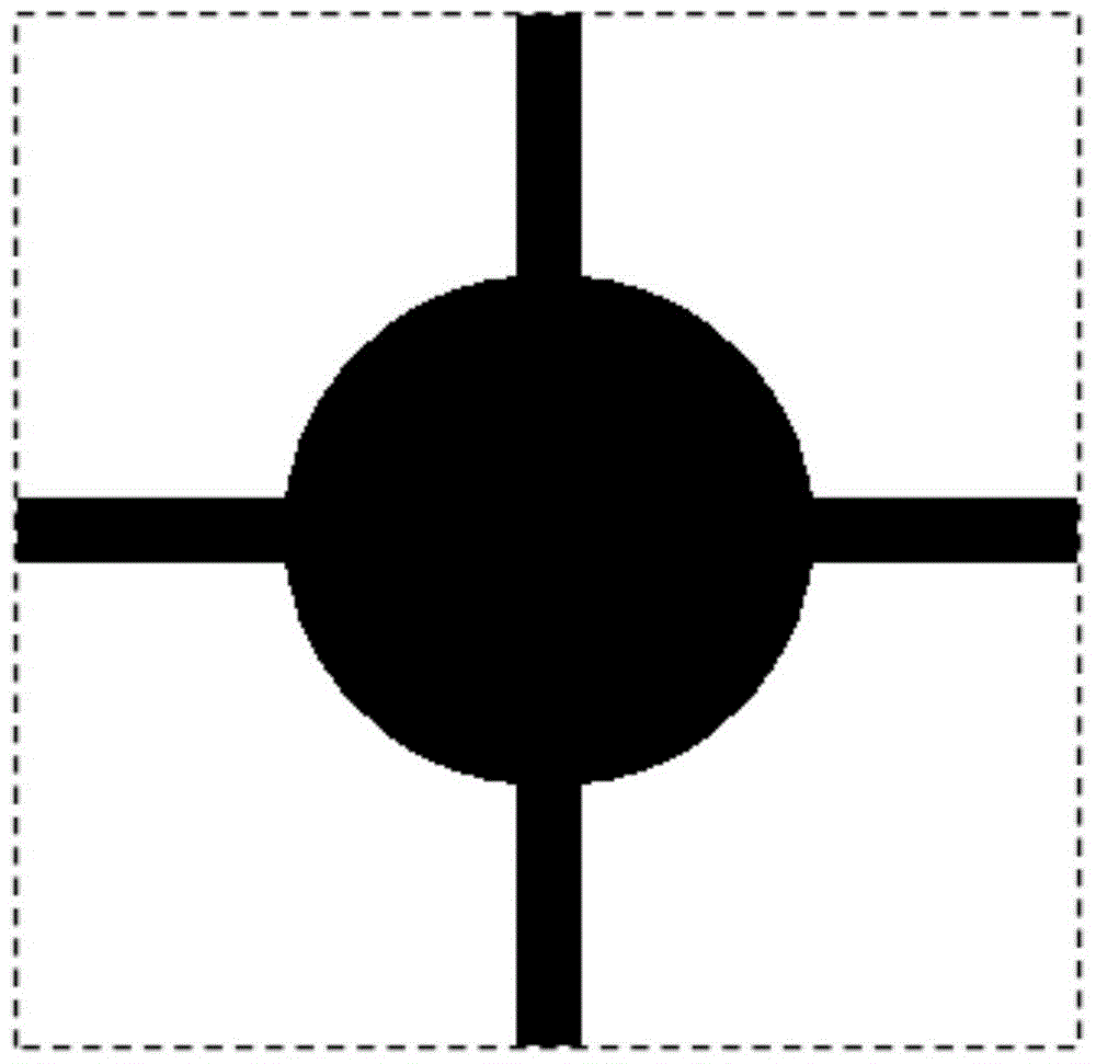
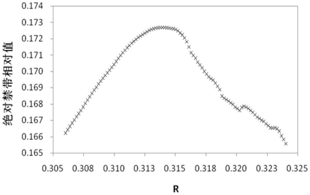
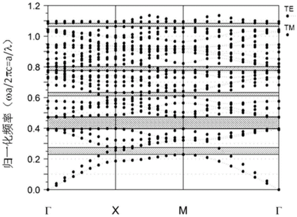
[0032] Embodiment 1. The high refractive index medium adopts silicon, the low refractive index medium is air, a=0.325, flat medium column width D=0.0558a=0.018135 micron, cylinder radius R=0.31392a=0.102024 micron, the absolute The range of forbidden band is (0.818722~0.688574), and the relative value of absolute forbidden band corresponds to 17.26755%.

Embodiment 2

[0033] Embodiment 2. The high refractive index medium adopts silicon, the low refractive index medium is air, a=0.45, the flat medium column width D=0.0558a=0.02511 micron, the cylinder radius R=0.31392a=0.141264 micron, the absolute The range of forbidden band is (1.133615~0.95341), and the relative value of absolute forbidden band corresponds to 17.26755%.

Embodiment 3

[0034] Embodiment 3. The high-refractive-index medium adopts silicon, the low-refractive-index medium is air, a=0.65, flat medium column width D=0.0558a=0.03627 micron, cylinder radius R=0.31392a=0.204048 micron, the obtained photonic crystal The range of the absolute forbidden band is (1.637445-1.377148), and the relative value of the absolute forbidden band corresponds to 17.26755%.


PUM


Abstract

Provided is a large absolute band-gap square-lattice photonic crystal based on cross-rod cylinders and circular cylinders, comprising a high-refractive-index medium cylinder and a low-refractive-index background medium cylinder. The high-refractive-index medium cylinder consists of a flat medium cylinder cross-rod connected to a circular medium cylinder, arranged in the direction of a cross; the cells of the photonic crystal structure are arranged according to the square lattice; the crystal constant of the square lattice is a; the width of the flat medium cylinder is 0.0558a, the external diameter of the cylinder is 0.31392a, and the relative value of the maximum absolute band gap is 17.26755%. The square lattice photonic crystal easily connects and couples different optical elements in an optical path, and different optical paths, facilitating reduced manufacturing costs; the photonic crystal structure has a large absolute band gap and is widely applicable to the design of large-scale integrated optical circuits.

Description

technical field [0001] The invention relates to a two-dimensional photonic crystal with wide absolute forbidden band. Background technique [0002] In 1987, E. Yablonovitch of Bell Laboratories in the United States was discussing how to suppress spontaneous emission, and S. John of Princeton University was discussing the photonic region and independently proposed the concept of photonic crystal (Photonic Crystal). A photonic crystal is a material structure in which dielectric materials are periodically arranged in space, and is usually an artificial crystal composed of two or more materials with different dielectric constants. [0003] In the frequency domain, for TE or TM waves propagating in any direction, the frequency interval where the electromagnetic field density of states is zero is defined as the TE or TM complete band gap of the photonic crystal, and the frequency interval where both TE and TM are completely forbidden is called a photonic crystal absolute ban. De...

Claims


Application Information

Patent Timeline
Patent Type & Authority Patents(China)
IPC IPC(8): G02B6/122
CPCG02B6/122
Inventor 欧阳征标王晶晶
Owner SHENZHEN UNIV
Why Eureka
Try Eureka