Large absolute bandgap square lattice photonic crystal based on three-link column and ring column

A technology of photonic crystals and square lattices, applied in the field of two-dimensional photonic crystals with wide absolute bandgap, can solve the problems of small absolute bandgap width, etc., and achieve the effects of easy connection and coupling, great convenience and flexibility, and simple optical path

Inactive Publication Date: 2016-01-20
SHENZHEN UNIV
View PDF2 Cites 0 Cited by
  • Summary
  • Abstract
  • Description
  • Claims
  • Application Information

AI Technical Summary

Problems solved by technology

[0005] Traditionally, in order to obtain a large relative forbidden band, non-square lattice structures such as triangular lattice and hexagonal lattice need to be used. However, in the integrated optical path of photonic crystals, the use of square lattice structure can make the optical path simple and easy to provide Integration, while the absolute band gap of the traditional square lattice photonic crystal is very small, so the formation of a square lattice photonic crystal with a large absolute band gap is the goal that people have been pursuing.

Method used


Image

  • Large absolute bandgap square lattice photonic crystal based on three-link column and ring column
  • Large absolute bandgap square lattice photonic crystal based on three-link column and ring column
  • Large absolute bandgap square lattice photonic crystal based on three-link column and ring column

Examples


Embodiment 1

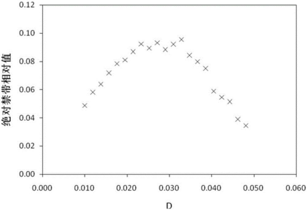
[0040] Embodiment 1. The high refractive index medium adopts silicon, the low refractive index medium is air, a=0.325, the flat medium column width D=0.0286a=0.009295 microns, the outer diameter of the circular column R=0.286a=0.09295 microns, the circular column The inner diameter is 0.00093 microns, the absolute band gap range of the obtained photonic crystal is (0.769449~0.693378), and the relative value of the absolute band gap corresponds to 10.401486%.

Embodiment 2

[0041] Embodiment 2. The high refractive index medium adopts silicon, the low refractive index medium is air, a=0.45, the flat medium column width D=0.0286a=0.1287 microns, the circular column outer diameter R=0.286a=0.1287 microns, and the circular column The inner diameter is 0.001287 microns, the absolute band gap range of the obtained photonic crystal is (1.65391~0.960061), and the relative value of the absolute band gap corresponds to 10.401486%.

Embodiment 3

[0042] Embodiment 3. The high refractive index medium adopts silicon, the low refractive index medium is air, a=0.65, the flat medium column width D=0.0286a=0.01859 micron, the circular column outer diameter R=0.286a=0.1859 micron, the circular column The inner diameter is 0.001859 microns, the range of the absolute forbidden band of the obtained photonic crystal is (1.538899-1.386755), and the relative value of the absolute forbidden band is correspondingly 10.401486%.


PUM


Abstract

Provided is a large absolute band-gap square-lattice photonic crystal based on a three-rod cylinders and circular cylinders, comprising a high-refractive-index medium cylinder and a low-refractive-index background medium cylinder; the high-refractive-index medium cylinder consists of a flat medium cylinder three-rod connected to a circular medium cylinder; the flat medium cylinder is constituted by a horizontal flat medium, a vertical flat cylinder, and an oblique flat cylinder having a square lattice cellular horizontal lattice vector at an angle of 45° or 135°; the cells of the photonic crystal structure are arranged according to the square lattice; the crystal constant of the square lattice photonic crystal is a; the width (D) of the flat medium cylinder is 0.0286a, the outer diameter (R) of the circular cylinder is 0.286a; the ratio (T) of the difference between the inner and outer diameters of the circular cylinder to the circular outer diameter (R) is 0.99, corresponding to the relative value of the maximum absolute band gap being 10.401486%. The photonic crystal structure has a very large absolute band gap, and is widely applicable to the design of large-scale integrated optical circuits.

Description

technical field [0001] The invention relates to a two-dimensional photonic crystal with wide absolute forbidden band. Background technique [0002] In 1987, E. Yablonovitch of Bell Laboratories in the United States was discussing how to suppress spontaneous emission, and S. John of Princeton University was discussing the photonic region and independently proposed the concept of photonic crystal (Photonic Crystal). A photonic crystal is a material structure in which dielectric materials are periodically arranged in space, and is usually an artificial crystal composed of two or more materials with different dielectric constants. [0003] In the frequency domain, for TE or TM waves propagating in any direction, the frequency interval where the electromagnetic field density of states is zero is defined as the TE or TM complete band gap of the photonic crystal, and the frequency interval where both TE and TM are completely forbidden is called a photonic crystal absolute ban. De...

Claims


Application Information

Patent Timeline
Patent Type & Authority Patents(China)
IPC IPC(8): G02B1/02
CPCG02B6/122
Inventor 欧阳征标王晶晶
Owner SHENZHEN UNIV
Why Eureka
Try Eureka