Substrate with built-in electronic components

A technology for electronic components and built-in substrates, which is applied in the field of built-in substrates for electronic components, and can solve problems such as the influence of component functions and cracks

Active Publication Date: 2018-05-29
TAIYO YUDEN KK
View PDF4 Cites 0 Cited by
  • Summary
  • Abstract
  • Description
  • Claims
  • Application Information

AI Technical Summary

Problems solved by technology

Therefore, the stress caused by the thermal expansion or contraction of the upper surface layer will be directly transmitted to the fragile element body, causing damage such as cracks, which may affect the function of the element

Method used


Image

  • Substrate with built-in electronic components
  • Substrate with built-in electronic components
  • Substrate with built-in electronic components

Examples


no. 1 Embodiment approach ( pic 1

[0041] [The first embodiment ( figure 1 and figure 2 )]

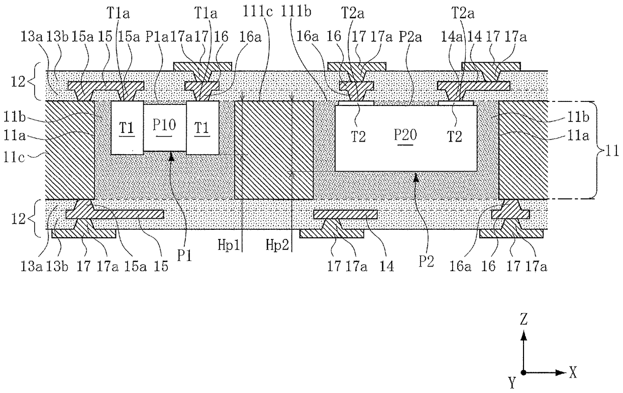
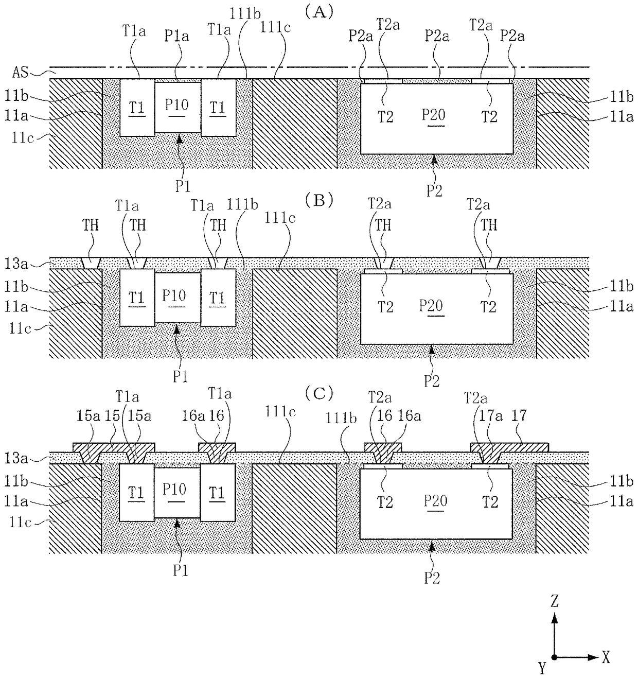
[0042] figure 1 It is a vertical cross-sectional view of the electronic component built-in substrate according to this embodiment. in addition, Figure 1 ~ Figure 3 The X-axis direction, Y-axis direction, and Z-axis direction in the graph represent three vertical (coordinate) axis directions, the X-axis direction and the Y-axis direction represent the horizontal direction, and the Z-axis direction represents the thickness direction (up-down direction).

[0043] First, explain figure 1The basic structure of the substrate with built-in electronic components is shown. The electronic component built-in substrate has: a component storage layer 11; The build-up layers 12 are respectively provided on the other surface (lower surface) perpendicular to the (thickness direction).

[0044] The component housing layer 11 has two electronic components P1 and P2, an insulating covering part 11b, and a base material 11c. The ...

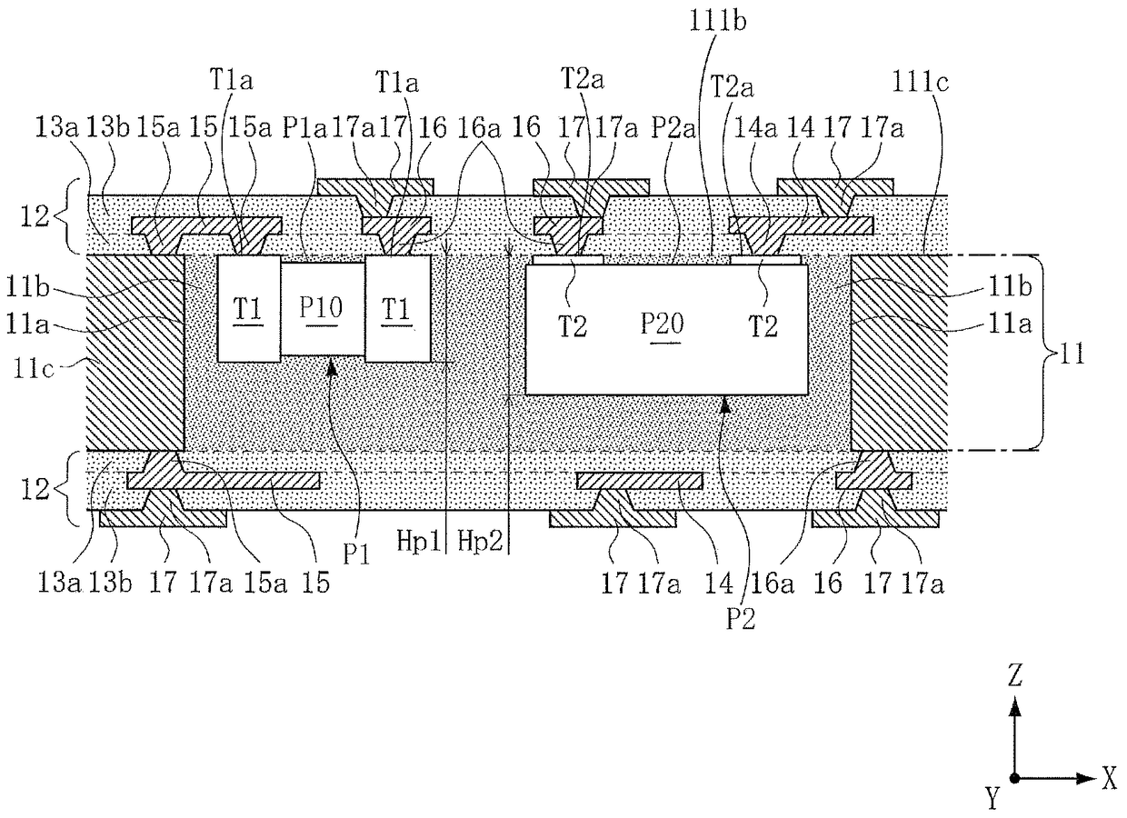
no. 2 Embodiment approach ( pic 3)

[0080] image 3 The electronic components shown are built into the substrate and figure 1 The shown electronic component built-in substrate differs in structure in that the component housing layer includes a plurality of electronic components accommodated in one cavity portion 11a. In addition, similarly to the first embodiment, the covering portion 11b and the electronic components P1, P2 are accommodated in the cavity portion 11a, and the covering portion 11b is filled with the two electronic components P1, P2 and the cavity portion. 11a between the gaps between the way and set. In addition, in the step of forming the component housing layer of the substrate with built-in electronic components (component placement step), in addition to inserting the two electronic components P1 and P2 into one cavity portion 11a and then filling the uncoated portion 11b, Except for the difference of the hardened material, the other processes are the same as those described above.

[0081]...


PUM


Abstract

The present invention provides an electronic component built-in substrate capable of preventing failure of the electronic component even when thermal expansion or thermal contraction occurs in an insulating material formed on the electronic component. The electronic component-embedded substrate has a component housing layer and a build-up layer. The component housing layer has: an electronic component including a terminal surface and a main body; an insulating covering portion including a first surface formed on the same plane as the terminal surface for covering the main body of the electronic component, and has the first coefficient of linear expansion. The build-up layer includes: an insulating layer which is in contact with the terminal surface and the first surface, is formed on the element housing layer, and has a second coefficient of linear expansion greater than the first coefficient of linear expansion; It is provided on the above-mentioned insulating layer and connected to the above-mentioned terminal surface.

Description

technical field [0001] The present invention relates to a multilayer structure electronic component built-in substrate (package substrate) built with electronic components. Background technique [0002] Electronic component built-in substrates generally have a structure in which conductive holes connected to terminals of the electronic component are provided on an insulating material formed on the surface of the electronic component, and a synthetic resin containing an insulating filler is used as the insulating material. In addition, the conduction hole part is formed by methods, such as irradiating laser light from the upper side of an insulating material, for example. [0003] For example, Patent Document 1 discloses an element-embedded substrate having an element-embedded resin layer having a side surface layer formed of a layer of the element-embedded resin layer lower than that of the chip element. The part of the upper surface is constituted; the upper surface layer ...

Claims


Application Information

Patent Timeline
Patent Type & Authority Patents(China)
IPC IPC(8): H05K1/02
CPCH05K1/185H05K3/4602H05K2201/0209H05K2201/068H05K2201/10636H05K2203/1469H01L24/19H01L2924/12042H01L2224/04105H01L2924/19105Y02P70/50H01L2924/00H05K1/0298H05K1/183
Inventor 杉山裕一猿渡达郎井上佑介宫崎政志
Owner TAIYO YUDEN KK
Why Eureka
Try Eureka