Antenna circuit, ic inlet, and ic tag

一种天线电路、插入物的技术,应用在非接触IC标签领域,能够解决制造工序增加等问题

Inactive Publication Date: 2007-06-06
LINTEC CORP
View PDF7 Cites 1 Cited by
  • Summary
  • Abstract
  • Description
  • Claims
  • Application Information

AI Technical Summary

Problems solved by technology

Furthermore, a step of forming a peeling layer with different peeling force is required, and there is a problem of increasing the number of manufacturing steps.

Method used


Image

  • Antenna circuit, ic inlet, and ic tag
  • Antenna circuit, ic inlet, and ic tag
  • Antenna circuit, ic inlet, and ic tag

Examples


manufacture example 1

[0089] (Manufacture of antenna circuit)

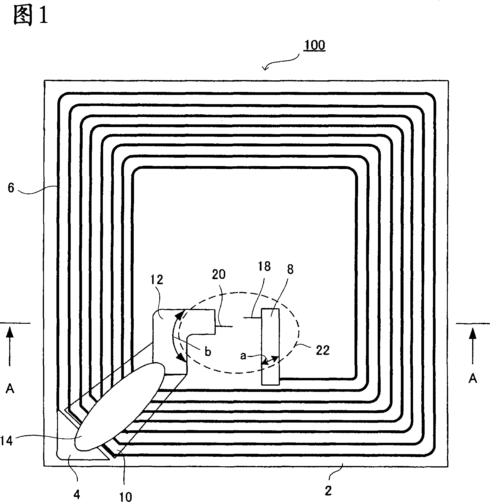
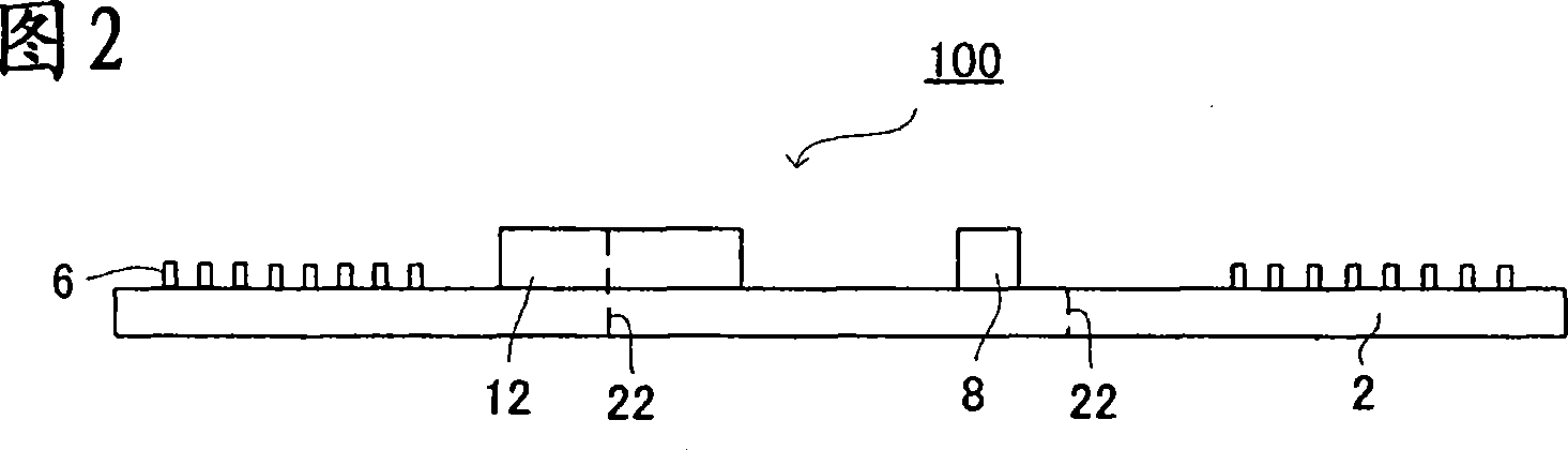
[0090] The antenna circuits 100 shown in FIGS. 1 and 2 are manufactured in groups of 20 by the method described below.

[0091] First, a resist pattern was printed by a screen printing method on the brand name Nika Flux (Cu / PET = 35 μm / 50 μm manufactured by Nikon Kogyo Co., Ltd.) in which copper foil and polyethylene terephthalate film (PET) were bonded. The resist pattern is made, and the planar coil circuit portion 6, the counter electrodes 8, 12, and the lead portions 18, 20 are used as one constituent unit, and 20 constituent units are arranged vertically and horizontally. The nicaflex printed with a resist pattern is etched to remove unnecessary copper foil portions, and the planar coil circuit 6, the counter electrodes 8, 12, and the lead portions 18, 20 are formed.

[0092] Then, a lead electrode 4 was formed with silver paste (DW250L-1 manufactured by Toyobo Co., Ltd.) on one end of the planar coil circuit portion 6 described above...

manufacture example 2

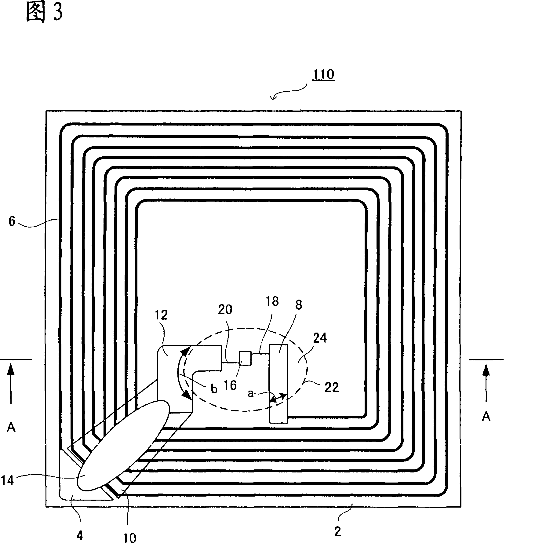
[0097] (Manufacturing of IC Insert)

[0098] An RFID-IC chip (I Code manufactured by Philips Co., Ltd.) was mounted on the antenna circuit manufactured as described above, and 20 IC inserts 110 having the configurations shown in FIGS. 3 and 4 were manufactured.

[0099] In actual installation, a flip chip mounter (FB30T-M manufactured by Kyushu Matsushita) is used. Furthermore, as an adhesive material, an anisotropic conductive adhesive (TAP0402E manufactured by Kyocera Co., Ltd.) was used, and thermocompression bonding was performed under the conditions of 220°C and 200 gf (1.96N) for 7 seconds.

Embodiment 1

[0101] (Manufacture of IC tags)

[0102] Using the above-mentioned IC insert, acrylic adhesive (manufactured by Lintec Co., Ltd., trade name, PA-T1) was coated with a thickness of 25 μm on a thin translucent paper coated with silicone resin as a release material ( The peel-off processing surface of Rintec Co., Ltd., trade name, 8KX) was bonded to the surface circuit forming surface of the IC insert. In this way, 20 IC tags having the same configuration as the IC tag 120 shown in FIG. 6 were manufactured.

[0103] The operation confirmation of the 20 manufactured IC tags was based on a Read / Write test using the I Code evaluation tool SLEV400 manufactured by Fisher.

[0104] Using SLEV400, after confirming that the IC tag is operating normally, stick the IC tag on the polypropylene resin board. After being removed from the board after 24 hours, as shown in Figure 7, the IC chip area remained on the polypropylene resin board, and the circuit was destroyed. All 20 damages were confirm...


PUM


Abstract

An IC inlet (110) comprises a substrate (2), a surface circuit including a plain coil circuit portion (6) formed on the substrate and opposed electrodes (8 and 12) individually connected with the two ends of the plain coil circuit portion (6), and an IC chip (16) packaged in connection with the opposed electrodes. The IC inlet further comprises a cut-away broken line (22) formed in at least a portion of the surface circuit and through the substrate and the surface circuit. An IC tag is manufactured by use of the IC inlet.

Description

Technical field [0001] The present invention relates to a non-contact IC tag used in personal authentication, business management, logistics management and the like. Background technique [0002] In recent years, non-contact IC tags that are mounted on persons and commodities (attached objects) to be managed to manage the distribution of these managed objects, etc. have become widespread. The IC tag can store data in the built-in IC chip. Furthermore, the IC tag exchanges information with the interrogator in a non-contact manner by means of radio waves, so that the data stored in the IC chip can be exchanged with the interrogator. [0003] As the application areas of IC tags, for example, it is built into the commuter coupons of various transportation agencies to manage the boarding zone and freight, and various fields such as the entry and exit management of people in enterprises, commodity inventory management, and logistics management. Various types of IC tags have been manufa...

Claims


Application Information

Patent Timeline
Patent Type & Authority Applications(China)
IPC IPC(8): G06K19/10B42D15/10G06K19/07G06K19/077
CPCG06K19/07749G06K19/0775H01Q7/04H01Q1/2225H01Q1/38
Inventor 松下大雅中田安一村上贵一
Owner LINTEC CORP
Why Eureka
Try Eureka