Check patentability & draft patents in minutes with Patsnap Eureka AI!

Method for protecting step slot, metal plating method for substrate of circuit board and circuit board

A technology of stepped grooves and circuit boards, which is applied in the direction of printed circuits, printed circuit manufacturing, electrical components, etc., can solve the problem of inability to effectively protect the pattern of stepped grooves, the long production process of pressing dry film or wet film, affecting the performance of circuit boards and Appearance and other issues, to achieve the effect of environmental protection, increase product market share, and low production cost

Active Publication Date: 2014-10-15
NEW FOUNDER HLDG DEV LLC +1
View PDF4 Cites 6 Cited by
  • Summary
  • Abstract
  • Description
  • Claims
  • Application Information

AI Technical Summary

Problems solved by technology

[0003] Defects in related technologies: the traditional pressed dry film or wet film production process is long and costly, the height difference of the stepped groove is easily damaged after being covered with dry film, and the graphics in the stepped groove cannot be effectively protected, and the inner layer is stepped The solder mask of the slotted window will easily lead to darker color after the subsequent production process, which will affect the performance and appearance of the circuit board

Method used


Image

  • Method for protecting step slot, metal plating method for substrate of circuit board and circuit board
  • Method for protecting step slot, metal plating method for substrate of circuit board and circuit board
  • Method for protecting step slot, metal plating method for substrate of circuit board and circuit board

Examples


Embodiment Construction

[0025] In order to understand the above-mentioned purpose, features and advantages of the present invention more clearly, the present invention will be further described in detail below in conjunction with the accompanying drawings and specific embodiments. It should be noted that, in the case of no conflict, the embodiments of the present application and the features in the embodiments can be combined with each other.

[0026] In the following description, many specific details are set forth in order to fully understand the present invention. However, the present invention can also be implemented in other ways than described here. Therefore, the protection scope of the present invention is not limited by the specific implementation disclosed below. Example limitations.

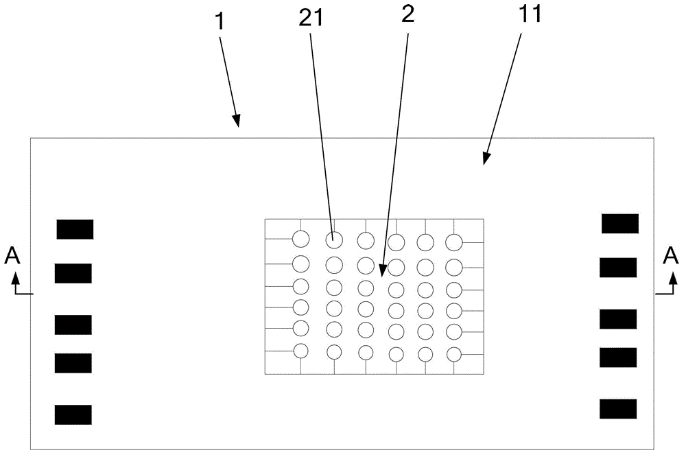
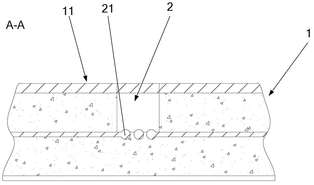
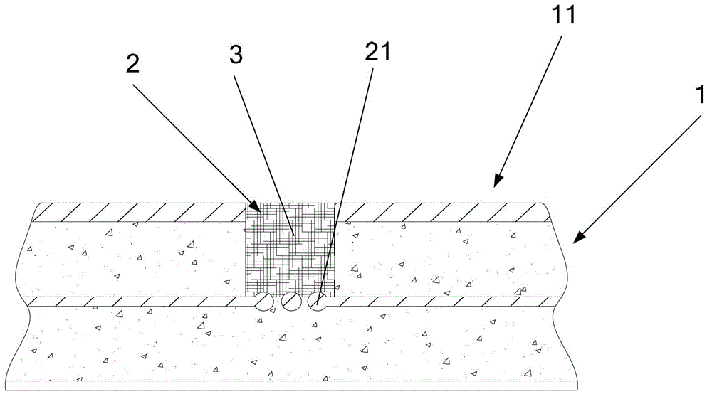
[0027] The method for protecting the stepped groove provided by the invention, such as Figure 1 to Figure 7 shown, including:

[0028] Step 101, performing surface treatment on the circuit board substrate ...


PUM


Abstract

The invention provides a method for protecting a step slot, a metal plating method for a substrate of a circuit board and a circuit board. The method for protecting the step slot comprises the following steps: carrying out surface treatment on the substrate of the circuit board; carrying out selected wet film coating treatment on the step slot, and filling selected wet film into the step slot to a preset position; carrying out metallic coating on a board of the substrate of the circuit board and the selected wet film; and carrying out pattern transfer treatment on the board, preparing a circuit and removing metal plated on the selected wet film Inside the step slot. Through the above method, the selected wet film can form a protective layer in a specific area so as to strengthen binding force with a copper surface and guarantee that the pattern of the undersurface of the step slot and the circuit during the follow-up manufacturing process are not influenced. The manufacturing cost is low. Waste formed by follow-up film removal can be effectively minimized. The method is beneficial to environmental protection. Meanwhile, the case that height of the step slot influences pressed film quality is avoided, and reject ratio is minimized.

Description

technical field [0001] The invention relates to the field of printed circuit board production and manufacturing, in particular to a method for protecting stepped grooves, a metal plating method for circuit board substrates, and a circuit board. Background technique [0002] With the continuous development of electronic technology, various electronic products are gradually developing in the direction of multi-function, low energy consumption, and easy portability; In addition to increasing the wiring through dense lines, the method of extending some electronic devices into the board by using a ladder method to reduce the overall thickness after punching has been gradually formed. This kind of product design will form stepped grooves recessed in some areas of the circuit board, but it will bring greater challenges to the manufacturing process in the actual production process, and the traditional operation method has been difficult to meet its production requirements. The prod...

Claims


Application Information

Patent Timeline
IPC IPC(8): H05K3/00
Inventor 车世民李晋峰
Owner NEW FOUNDER HLDG DEV LLC
Features
  • R&D
  • Intellectual Property
  • Life Sciences
  • Materials
  • Tech Scout
  • Unparalleled Data Quality
  • Higher Quality Content
  • 60% Fewer Hallucinations
Learn More