
Carrier wave offset circuit based on RFID reader-writer, and RFID reader-writer

A reader-writer and carrier technology, applied in the field of circuits, can solve the problems of expensive vector modulation chips, difficult hardware design, and insignificant vector modulation effects.

Active Publication Date: 2014-10-29
SHENZHEN MARKTRACE
View PDF4 Cites 3 Cited by
  • Summary
  • Abstract
  • Description
  • Claims
  • Application Information

AI Technical Summary

Problems solved by technology

There are mainly two ways to implement the vector modulation circuit in this circuit design scheme, one is to use the existing vector modulation chip, and the other is to use the traditional vector modulation circuit; the disadvantage of the former is that the vector modulation chip is relatively expensive, and the single The price of the chip is more than 100 yuan, plus the combiner and isolator, which seriously increases the design cost, while the traditional vector modulation circuit is more complicated to implement, and the vector modulation effect is not obvious
On the other hand, the vector modulation algorithm is also relatively complicated, and requires two analog signals of I and Q to control
Therefore, although this design scheme can weaken and eliminate the interference of the leaked carrier, the overall design has the disadvantages of high hardware design cost, difficult hardware design, complex software control algorithm, and difficult debugging, and is not suitable for mass production.

Method used


Image

  • Carrier wave offset circuit based on RFID reader-writer, and RFID reader-writer
  • Carrier wave offset circuit based on RFID reader-writer, and RFID reader-writer
  • Carrier wave offset circuit based on RFID reader-writer, and RFID reader-writer

Examples


Embodiment Construction

[0018] In order to make the object, technical solution and advantages of the present invention clearer, the present invention will be further described in detail below in conjunction with the accompanying drawings and embodiments. It should be understood that the specific embodiments described here are only used to explain the present invention, not to limit the present invention.

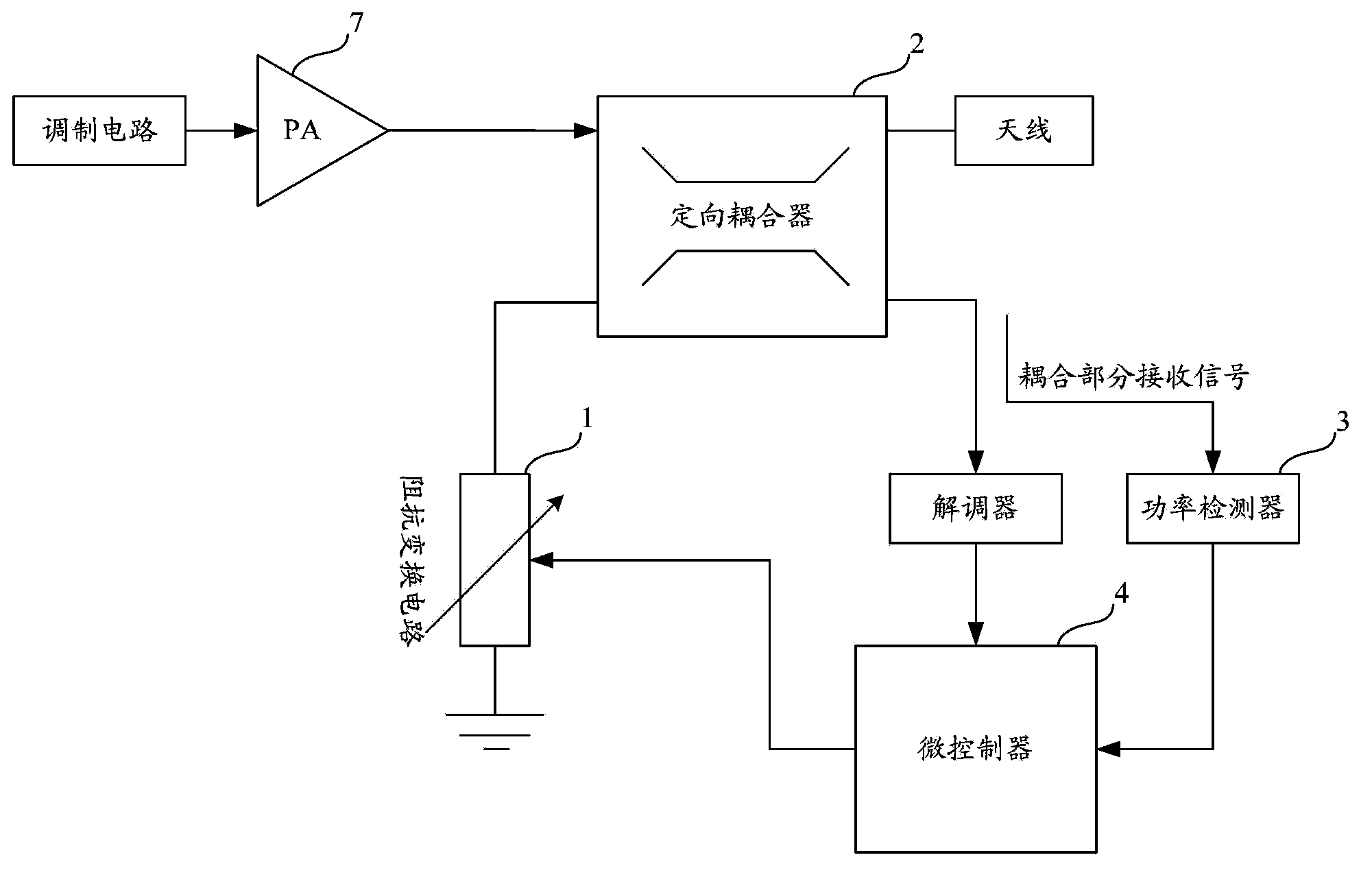
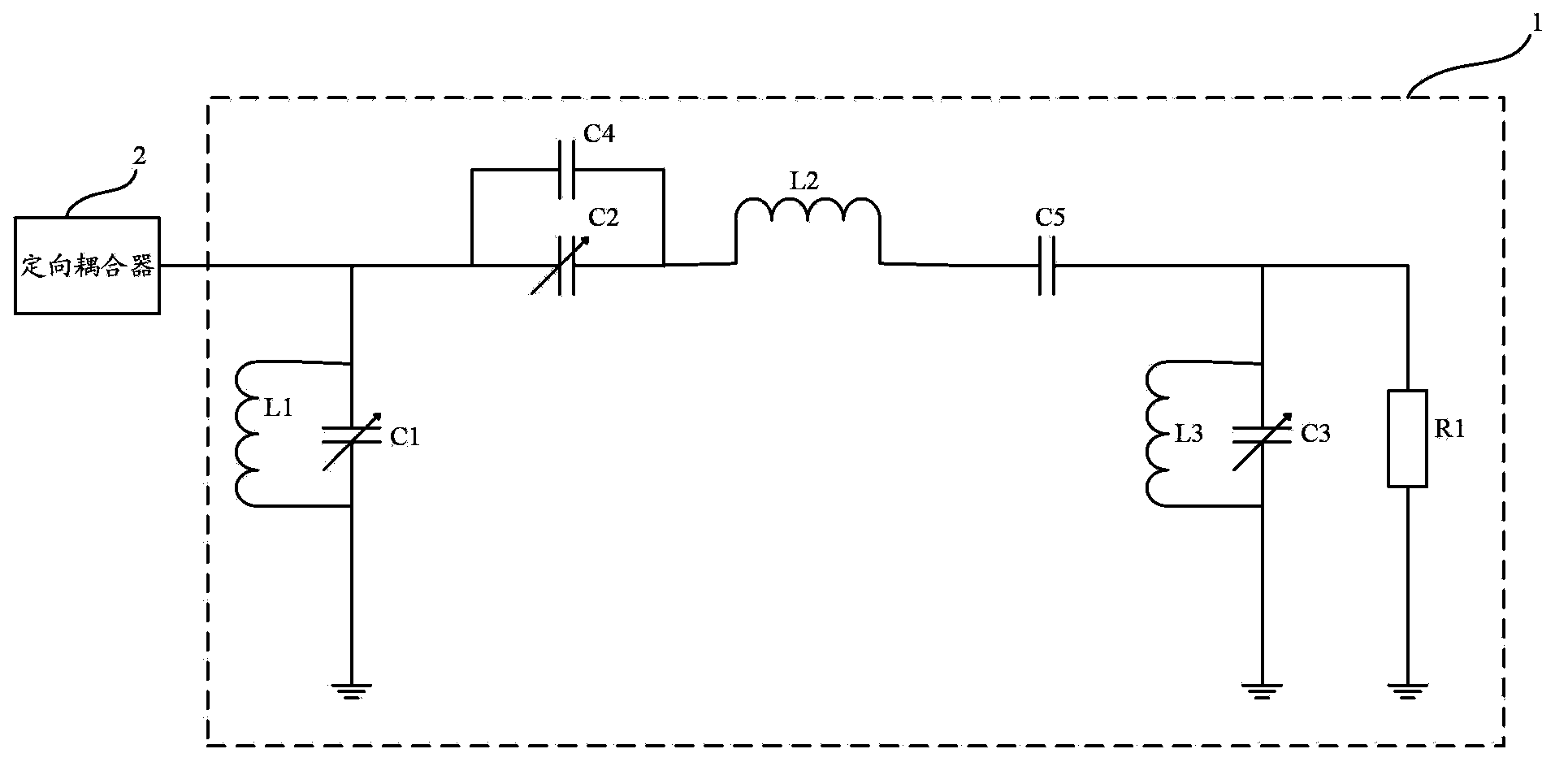
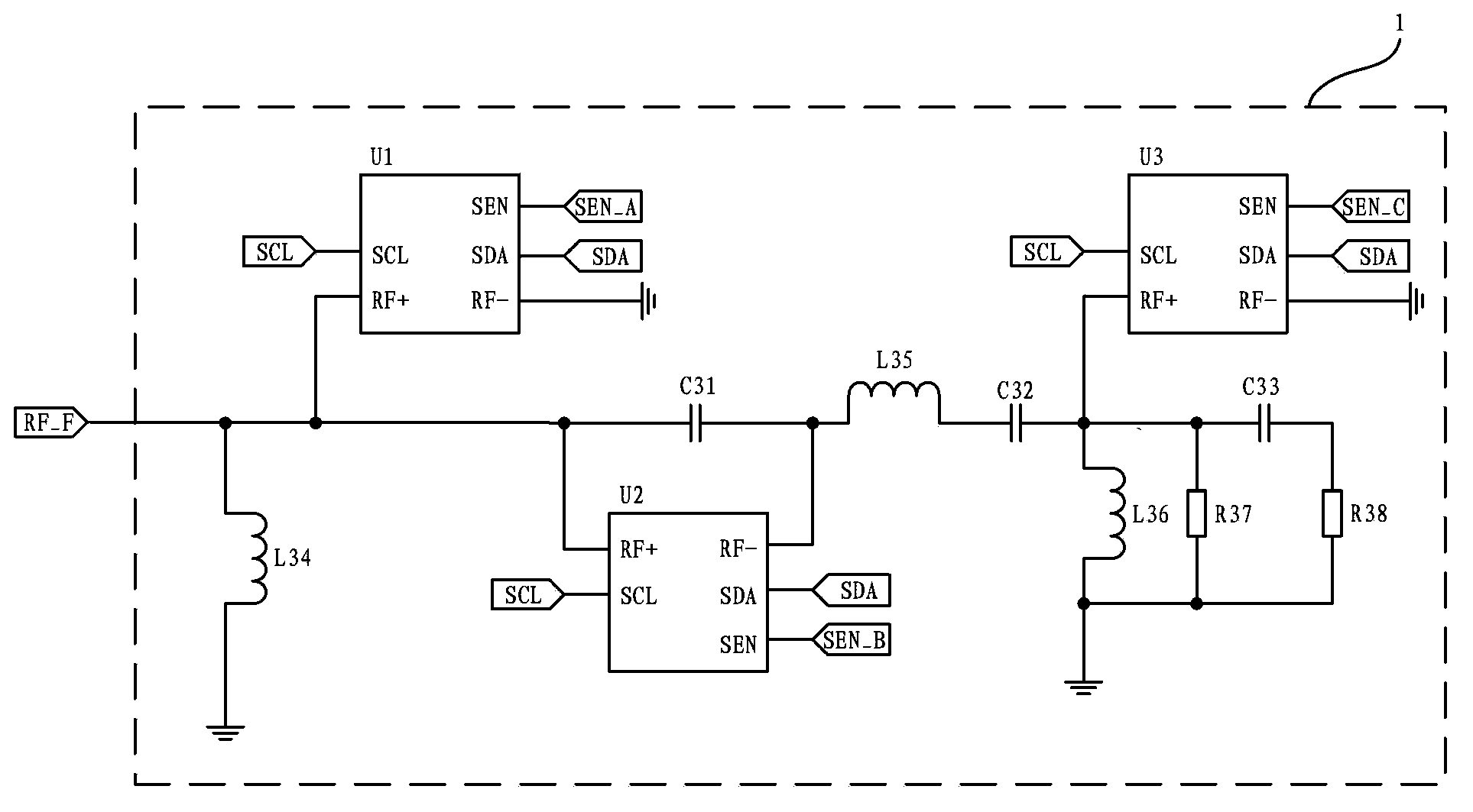
[0019] figure 1 The structure of the carrier cancellation circuit based on the RFID reader-writer provided by the embodiment of the present invention is shown. For the convenience of description, only the parts related to the embodiment of the present invention are shown, and the details are as follows.

[0020] A kind of carrier cancellation circuit based on RFID reader-writer, described carrier cancellation circuit based on RFID reader-writer comprises the modulation circuit for generating carrier signal, described carrier cancellation circuit based on RFID reader-writer is connected with antenna...


PUM


Abstract

The invention is applicable to the field of circuits and particularly relates to a carrier wave offset circuit based on an RFID reader-writer and the RFID reader-writer. In a work process of the RFID reader-writer, a controller adjusts the impedance of an impedance conversion circuit so as to adjust reception signals received by a demodulator. When a power detected by a power detector is lowest, it is represented that an offset effect of reflection signals of the impedance conversion circuit on leakage carrier wave signals are optimal so that it is easier for the demodulator to demodulate correct tag signals.

Description

technical field [0001] The invention belongs to the field of circuits, in particular to a carrier cancellation circuit based on an RFID reader-writer and the RFID reader-writer. Background technique [0002] As we all know, during the working process of the UHF RFID reader, when the electronic tag returns the signal to the reader, the reader also needs to transmit a carrier signal to provide energy to the electronic tag. Since the carrier signal emitted by the reader is very strong, it is inevitable that a part of the carrier signal will leak into the receiving channel. This part of the leaked carrier signal is much larger than the return signal of the tag, resulting in a decrease in the receiving sensitivity of the reader. In order to overcome this problem in recent years, carrier cancellation technology has appeared in the field of UHF technology. The principle of the method is to generate a signal with the same amplitude and opposite phase as the leaked carrier and add i...

Claims


Application Information

Patent Timeline
IPC IPC(8): G06K17/00
Inventor 高军刁尚华李荣海
Owner SHENZHEN MARKTRACE
Learn More