Quad flat no-lead package
A square, flat, leadless technology, applied to electrical components, electrical solid devices, circuits, etc., can solve the problem that QFN packages are easily damaged
- Summary
- Abstract
- Description
- Claims
- Application Information
AI Technical Summary
Problems solved by technology
Method used
Image

Examples
Embodiment 1
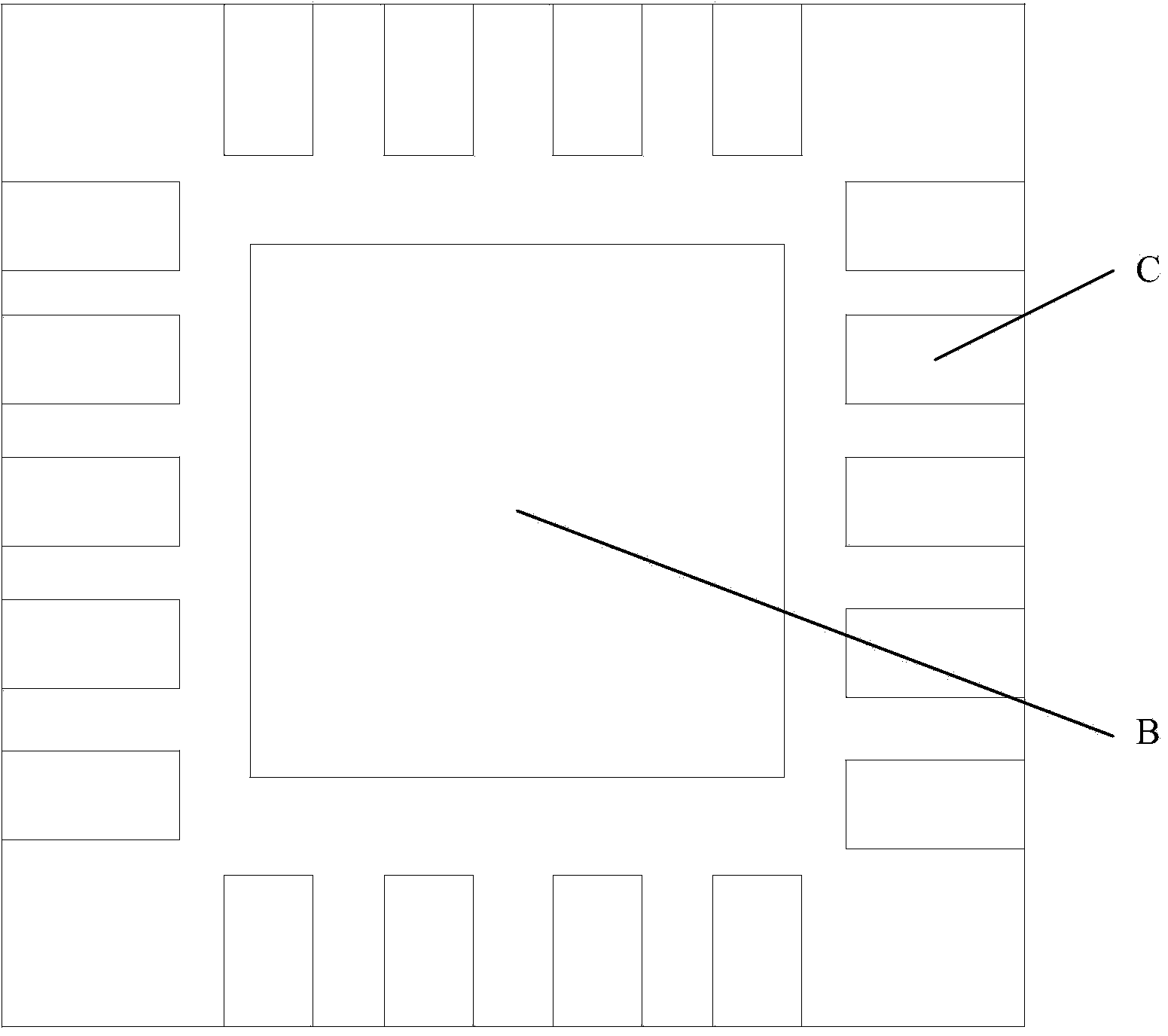
[0037] see figure 2 , which is a top view corresponding to Embodiment 1 of the QFN package provided by the present invention.
[0038] The QFN package provided by the present invention includes: an exposed pad B, an electrode contact C and a reinforced connection pad A;
[0039] The exposed pad B is located at the center of the bottom of the QFN package;
[0040] It should be noted that the exposed pad B has a larger area.
[0041] The electrode contacts C are arranged around the periphery of the QFN package;
[0042] It should be noted that the number of electrode contacts on opposite sides is the same. There are no electrode contacts on the four corners of the QFN package.
[0043] The QFN package can be square or rectangular.
[0044] The four corners of the QFN package are respectively provided with one of the enhanced connection pads A.
[0045] It can be understood that a total of four enhanced connection pads A are provided at the four corners of the QFN package....
Embodiment 2
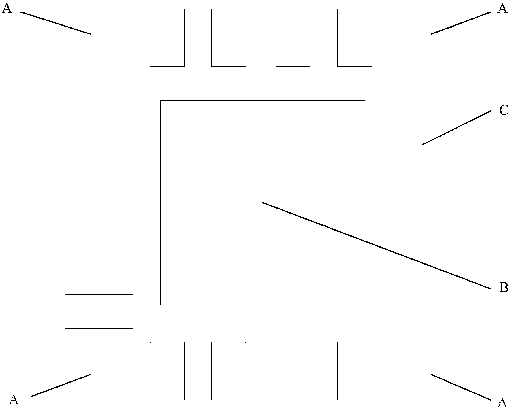
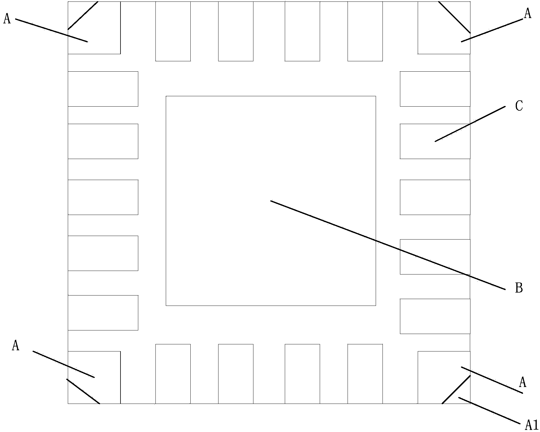
[0048] see image 3 , which is a top view corresponding to Embodiment 2 of the QFN package provided by the present invention.
[0049] In order to facilitate processing and cutting, the top of the four corners in the QFN package provided in this embodiment can reserve a triangular area, such as image 3 The four corners of the four reinforced connection pads A shown are reserved for a triangular area A1.
[0050] It should be noted that the enhanced connection pad A may be conductive or non-conductive according to the functional requirements of the actual chip.
[0051] In the QFN package provided in this embodiment, a triangular area is reserved at the four corners of the QFN package, and the triangular area is a filling area reserved for the boundary between the reinforced connection pad and the plastic-encapsulated QFN package. When the relatively large QFN package frame is divided into individual QFN packages, the burr caused by the enhanced connection pad can be avoided...
Embodiment 3
[0053] see Figure 4-5 , which is a front sectional view corresponding to Embodiment 3 of the QFN package provided by the present invention.
[0054] This figure is the main cross-sectional view, and the exposed pad B and electrode contact C of the QFN package can be seen.
[0055] In the QFN package provided in this embodiment, a bottom trench D is provided at the bottom of the exposed pad B.
[0056]It can be understood that, the bottom trench D divides the bottom of the exposed pad B into different regions; or the bottom trench D divides the bottom of the exposed pad B into different regions.
[0057] in addition, Figure 4 Among them, F is chip bonding (bonding line), E is bare chip, H is side climbing tin, and G is PCB.
[0058] Climbing tin H on the side can increase the connection between the QFN package and the PCB, making the connection between the two more reliable.
[0059] see Figure 6 , which is a top view corresponding to Embodiment 3 provided by the presen...
PUM
 Abstract
Description
Claims
Application Information
 - R&D Engineer
- R&D Manager
- IP Professional
- Industry Leading Data Capabilities
- Powerful AI technology
- Patent DNA Extraction
Browse by: Latest US Patents, China's latest patents, Technical Efficacy Thesaurus, Application Domain, Technology Topic.
© 2024 PatSnap. All rights reserved.Legal|Privacy policy|Modern Slavery Act Transparency Statement|Sitemap