Array substrate, display panel and display device

An array substrate and matrix technology, applied in the display field, can solve problems such as uneven brightness of odd and even rows, skewed polarizers, horizontal stripes of liquid crystal display devices, etc., and achieve the effect of avoiding horizontal stripes

Active Publication Date: 2018-01-12
SHANGHAI AVIC OPTOELECTRONICS +1
View PDF9 Cites 0 Cited by
  • Summary
  • Abstract
  • Description
  • Claims
  • Application Information

AI Technical Summary

Problems solved by technology

In the process of making a liquid crystal display device, when the rubbing alignment direction deviates during rubbing or the polarizer is skewed when it is attached, uneven brightness between odd and even lines will appear during display, which will lead to liquid crystal display The device produces stripes

Method used


Image

  • Array substrate, display panel and display device
  • Array substrate, display panel and display device
  • Array substrate, display panel and display device

Examples


Embodiment 1

[0046] Based on the above description, Embodiment 1 of the present invention provides the following solution.

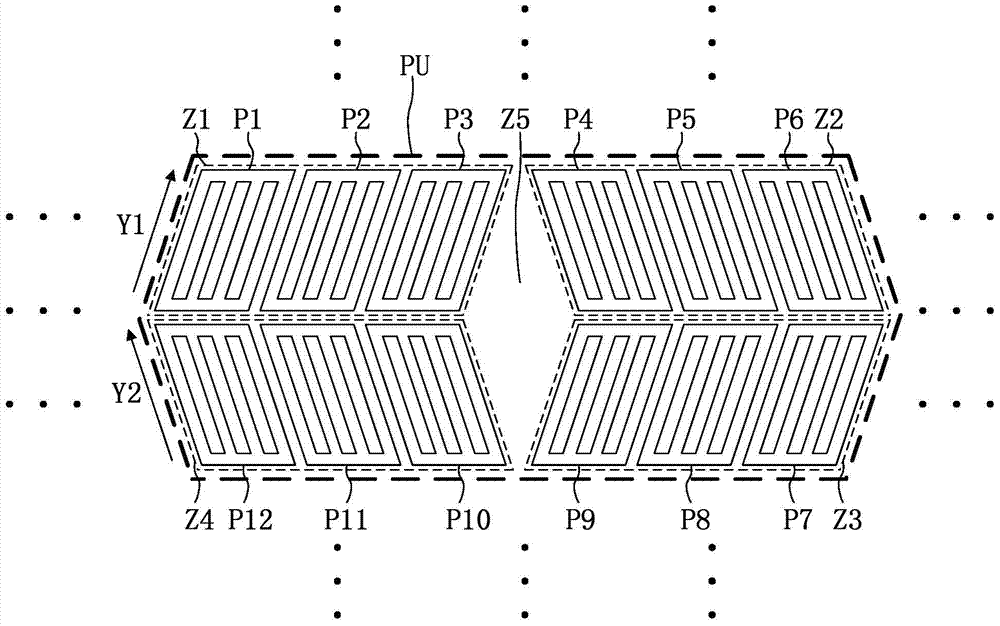
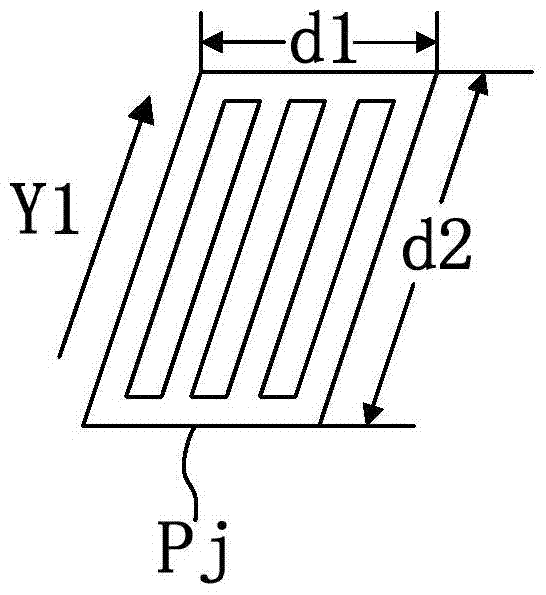
[0047] Embodiment 1 of the present invention provides an array substrate. Figure 1b It is a schematic structural diagram of an array substrate provided in Embodiment 1 of the present invention. see Figure 1b, the array substrate includes: a plurality of pixel units PU, the pixel unit PU includes a 2×2 sub-pixel region matrix, and the 2×2 sub-pixel region matrix includes a first sub-pixel region Z1, a second sub-pixel region arranged in sequence The pixel area Z2, the third sub-pixel area Z3 and the fourth sub-pixel area Z4; each of the sub-pixel areas includes three sub-pixel electrodes; each of the sub-pixel electrodes includes a strip electrode; the first sub-pixel Each of the zone Z1 and the third sub-pixel zone Z3 has at least one sub-pixel electrode in which the strip electrode is parallel to the first direction Y1; the second sub-pixel zone Z2 and the fourt...

Embodiment 2

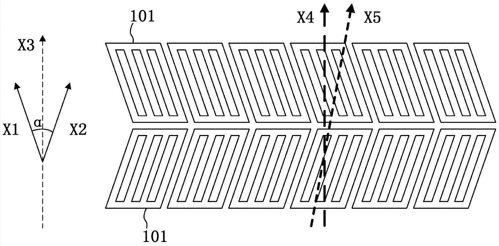
[0059] exist Figure 1b In the pixel unit shown, the strip electrodes in all the sub-pixel electrodes in the first sub-pixel area Z1 and the third sub-pixel area Z3 are parallel to the first direction Y1, and the second sub-pixel area Z2 and the fourth sub-pixel area The strip electrodes in all the sub-pixel electrodes in Z4 are parallel to the second direction Y2. For such a pixel unit, among the sub-pixel electrodes in the same row, the number of sub-pixel electrodes where the strip electrodes parallel to the first direction Y1 are located and the number of sub-pixel electrodes where the strip electrodes parallel to the second direction Y2 are located equal, if the rubbing alignment direction deviates during rubbing or the polarizer is skewed during attachment, then the brightness corresponding to the sub-pixel electrodes in the same row presents a relatively uniform distribution of bright and dark, and the adjacent two sub-pixel electrodes in the same column The parallel d...

Embodiment 3

[0063] Figure 3a It is a schematic structural diagram of a pixel unit provided by Embodiment 3 of the present invention. see Figure 3a , on the basis of the structure of the array substrate described in Embodiment 1, the pixel unit on the array substrate of this embodiment may further be: the four sub-pixel regions respectively include three sub-pixel electrodes, each of the four sub-pixel regions It includes a 1×3 sub-pixel electrode matrix; each of the first sub-pixel region Z1 and the third sub-pixel region Z3 has a sub-pixel electrode in which the strip electrodes are parallel to the first direction Y1; Each of the second sub-pixel region Z2 and the fourth sub-pixel region Z4 has one sub-pixel electrode in which the strip electrode is parallel to the second direction Y2; the pixel unit includes two first regions ( Z5 and Z6).

[0064] see Figure 3a Specifically, the strip electrodes in the first subpixel electrode P1 and the seventh subpixel electrode P7 are paralle...


PUM


Abstract

An array substrate including a plurality of pixel units each including a 2×2 sub-pixel area matrix, where each of the sub-pixel areas includes three sub-pixel electrodes. The strip electrode of at least one of the sub-pixel electrodes from each of the first sub-pixel area and the third sub-pixel area is parallel to a first direction, and the strip electrode of at least one of the sub-pixel electrodes from each of the second sub-pixel area and the fourth sub-pixel area is parallel to a second direction. The first direction intersects with the second direction. Also, a first area is defined by the sub-pixel electrodes including the strip electrodes parallel to the first direction and the sub-pixel electrodes including the strip electrodes parallel to the second direction, and the first area is provided with a sub-pixel electrode.

Description

technical field [0001] The present invention relates to the field of display technology, in particular to an array substrate, a display panel and a display device. Background technique [0002] Liquid crystal display devices have the advantages of thinness, low power consumption and low radiation, and are widely used in various fields. With the development of liquid crystal display technology, the display effect of liquid crystal display devices has been continuously improved. [0003] In the prior art liquid crystal display device, the strip electrodes in each row of pixel electrodes on the array substrate adopt a pseudo-double-domain structure arrangement, that is, for the strip electrodes in any two adjacent rows of pixel electrodes, one row The parallel direction of the strip-shaped electrodes is different from that of the other row of strip-shaped electrodes. In the process of making a liquid crystal display device, when the rubbing alignment direction deviates during...

Claims


Application Information

Patent Timeline
Patent Type & Authority Patents(China)
IPC IPC(8): G02F1/1343
CPCG02F1/133707G02F1/134336G02F1/134345G02F1/13439H01L27/124H01L29/40H01L29/786
Inventor 金慧俊曹兆铿林珧李岩松王苗苗
Owner SHANGHAI AVIC OPTOELECTRONICS
Why Eureka
Try Eureka