

A method for preparing plasma nitride gate dielectric layer
A gate dielectric layer, plasma nitriding technology, applied in semiconductor/solid-state device manufacturing, electrical components, circuits, etc., can solve the problem that the equivalent thickness of oxide cannot be reduced, the gate leakage cannot be effectively reduced, and the reliability of the device is affected. problem, to achieve the effect of reducing leakage current density, increasing nitrogen content, and improving reliability
- Summary
- Abstract
- Description
- Claims
- Application Information
AI Technical Summary
Problems solved by technology
Method used
Image

Examples
Embodiment Construction
[0031] The specific implementation of the present invention will be described in more detail below in conjunction with the schematic diagram. According to the following description and claims, the advantages and features of the present invention will be clearer. It should be noted that the drawings are in a very simplified form and all use imprecise proportions, which are only used to conveniently and clearly assist in explaining the purpose of the embodiments of the present invention.
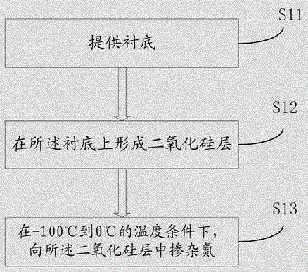
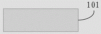
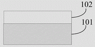
[0032] The present invention provides a method for preparing a plasma nitrided gate dielectric layer, such as figure 1 Shown is a schematic flow diagram of a method for preparing a plasma nitrided gate dielectric layer according to an embodiment of the present invention. Figure 2 ~ Figure 4 It is a schematic diagram of a structure formed by preparing a plasma nitrided gate dielectric layer according to the above process in an embodiment of the present invention.
[0033] It includes the following...
PUM
 Abstract
Description
Claims
Application Information