High-density multichannel waveguide network
A multi-channel, high-density technology, used in waveguide-type devices, electrical components, connecting devices, etc., can solve the problems of large arrangement space and long waveguide links, achieve flexible assembly and disassembly, reduce the difficulty of processing and molding, realize The effect of miniaturization
- Summary
- Abstract
- Description
- Claims
- Application Information
AI Technical Summary
Problems solved by technology
Method used
Image

Examples
Embodiment Construction
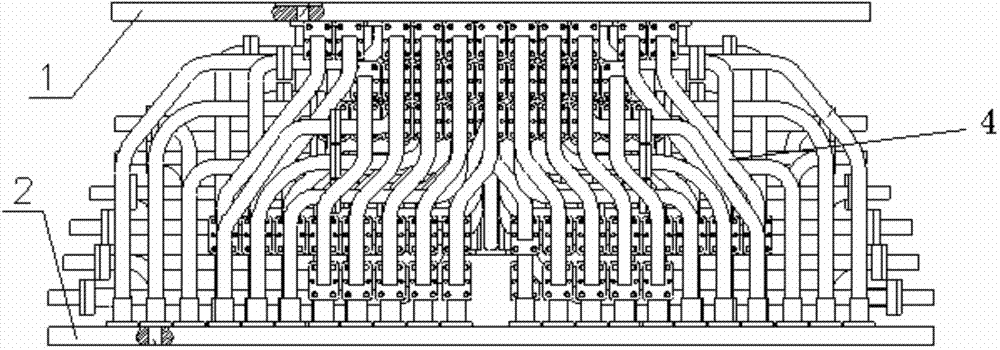
[0024] The existing transitional waveguide network is usually composed of only a few waveguide links, and the layout space is relatively large, the spatial layout is relatively simple, and the waveguide direction is relatively simple. In this way, in the actual use process, if a certain waveguide fails and needs to be replaced, it is a difficult matter. Moreover, the large space occupation also severely limits the application occasions. How to arrange multiple waveguide links in a small space, and how to repair and replace waveguide links conveniently and quickly when a fault occurs has become a problem that needs to be solved.
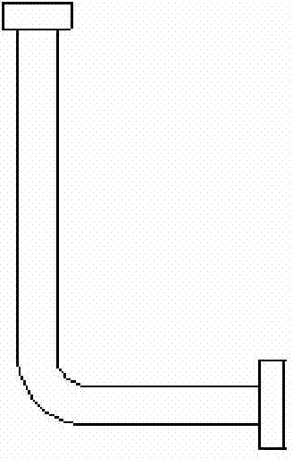
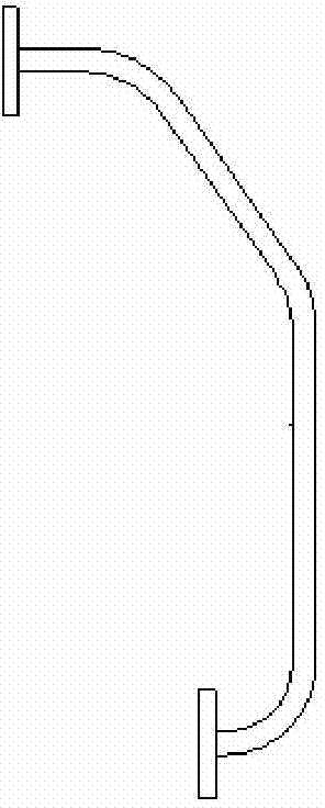
[0025] In view of the deficiencies of existing technologies, such as figure 1 As shown, the present invention provides a high-density multi-channel waveguide network, comprising: upper flange 1, lower flange 2, top layer waveguide link 3, middle layer waveguide link 4 and bottom layer waveguide link 5; upper flange 1 and the lower flange 2 are both c...
PUM
 Abstract
Description
Claims
Application Information