Array substrate, display panel, display device and repairing method for display panel

A technology for array substrates and display panels, which can be applied to instruments, semiconductor devices, optics, etc., and can solve problems such as smaller aperture ratios

Inactive Publication Date: 2015-01-21
BOE TECH GRP CO LTD +1
View PDF3 Cites 8 Cited by
  • Summary
  • Abstract
  • Description
  • Claims
  • Application Information

AI Technical Summary

Problems solved by technology

[0004] Embodiments of the present invention provide an array substrate, a display panel, a display device, and a repair method for a display panel, so as to solve the problem that the aperture ratio becomes smaller when the existing array substrate repairs poor light leakage.

Method used


Image

  • Array substrate, display panel, display device and repairing method for display panel
  • Array substrate, display panel, display device and repairing method for display panel

Examples


Embodiment 1

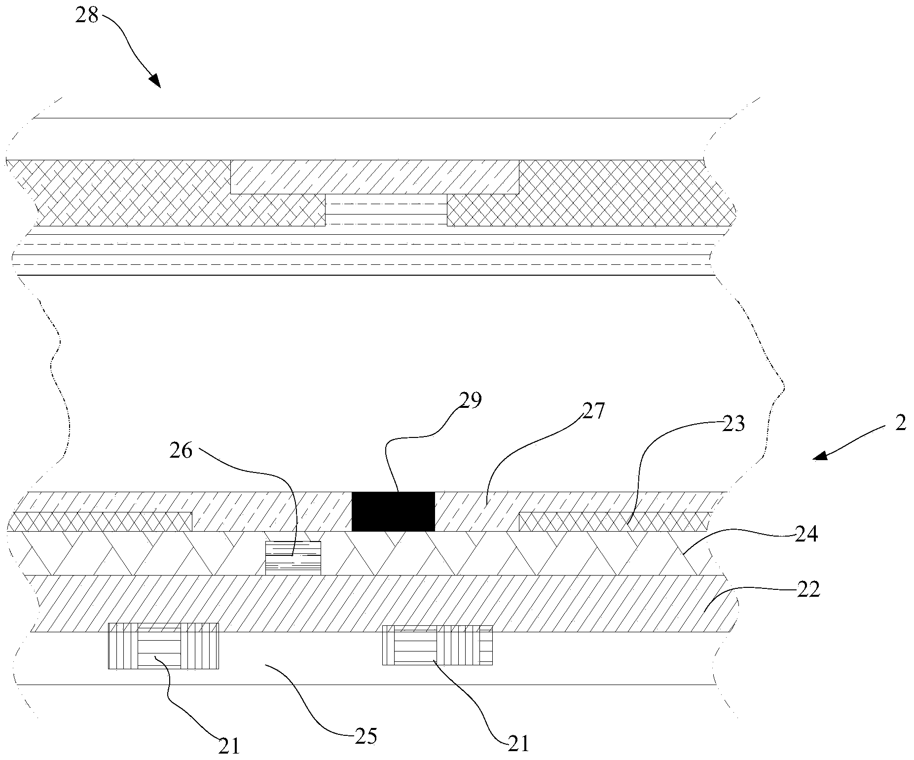
[0023] see figure 2 , this embodiment provides an array substrate 2, the array substrate 2 includes a functional layer, and also includes a photochromic layer 27, the photochromic layer 27 is arranged on the functional layer, when the array substrate 2 appears When the light leakage is poor, the light blocking layer 29 is formed by irradiating the photochromic layer 27 with light.

[0024] In the array substrate 2 provided in the embodiment of the present invention, since the photochromic layer 27 is provided on the functional layer, when it is found that the array substrate 2 has poor light leakage during the inspection process, the photochromic layer 27 can be irradiated with light. The color-changing layer 27 makes the photochromic layer 27 form the light-shielding layer 29 , so as to repair the light leakage defect of the array substrate 2 .

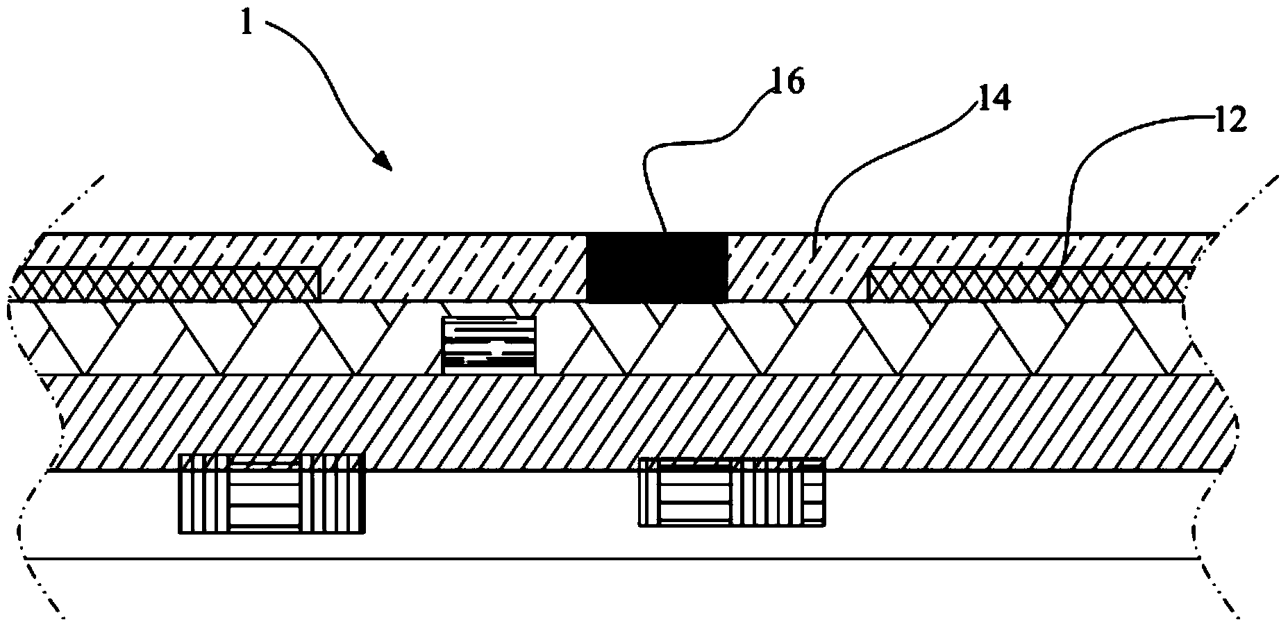
[0025] As a preferred embodiment of the present invention, see figure 1 , the photochromic layer 14 can be disposed on the pixel...

Embodiment 2

[0032] This embodiment provides a display panel, which includes the above-mentioned array substrate 2, and the array substrate 2 includes a functional layer. Since the functional layer is provided with a photochromic layer 27, it is found that the array substrate 2 has light leakage during the inspection process. In case of failure, the photochromic layer 27 can be irradiated with light, so that the photochromic layer forms a light blocking layer 29, thereby repairing the defective light leakage of the array substrate 2, and further repairing the defective light leakage of the display panel.

[0033] see figure 2 The above-mentioned display panel may also include a counter substrate 28 that is co-located with the array substrate 2, and when the display panel has poor light leakage, the photochromic layer 27 is irradiated with light to form a light-blocking layer 29, so that The light leakage defect of the display panel has been fixed. Since the display panel includes the abo...

Embodiment 3

[0035] This embodiment provides a display device, which includes the above-mentioned display panel. The display panel includes the above-mentioned array substrate 2, and the array substrate 2 includes a functional layer. Since the functional layer is provided with a photochromic layer 27, when the array substrate 2 is found to have poor light leakage during the inspection process, the photochromic layer can be irradiated with light. 27, making the photochromic layer 27 form a light blocking layer 29, thereby repairing the defective light leakage of the array substrate 2, and further repairing the defective light leakage of the display device.


PUM


Abstract

The invention discloses an array substrate, a display panel, a display device and a repairing method for the display panel, and relates to the technical field of display. The method is invented for solving the problem that when poor light leakage of an existing array substrate is repaired, the aperture opening ratio is decreased. The array substrate comprises a function layer and a photochromic layer arranged on the function layer. When poor light leakage of the array substrate occurs, the photochromic layer forms a light shielding layer through light illumination.

Description

technical field [0001] The invention relates to the field of display technology, in particular to an array substrate, a display panel, a display device and a repair method for the display panel. Background technique [0002] With the development of display manufacturing technology, TFT-LCD (Thin Film Transistor Liquid Crystal Display) occupies a dominant position in the current flat panel display market due to its small size, low power consumption, and no radiation. Array substrates are important components in liquid crystal display devices. Among them, the aperture ratio is an important index for evaluating the array substrate. The larger the aperture ratio, the higher the transmittance of the array substrate, the higher the brightness of the TFT-LCD, and the better the display effect of the liquid crystal display. [0003] Array substrates often have poor light leakage. At this stage, the method of widening the black matrix is ​​usually used to solve the problem of poor ...

Claims


Application Information

Patent Timeline
IPC IPC(8): G02F1/1335G02F1/136
CPCG02F1/1309G02F1/133512G02F1/136209G02F1/136259G02F1/136286G02F2201/123G02F2202/02G02F2202/14G02F2203/05G02F1/136222H01L27/124H01L29/78633
Inventor 颜莎宁石博
Owner BOE TECH GRP CO LTD
Why Eureka
Try Eureka