Light-emitting device containing flattened anisotropic colloidal semiconductor nanocrystals and processes for manufacturing such devices

A nanocrystal, anisotropic technology, applied in the field of light-emitting devices containing anisotropic planar colloidal semiconductor nanocrystals and its manufacturing, can solve the problems of not allowing and not allowing to optimize the energy efficiency of devices

Active Publication Date: 2015-01-21
NEXDOT
View PDF6 Cites 10 Cited by
  • Summary
  • Abstract
  • Description
  • Claims
  • Application Information

AI Technical Summary

Problems solved by technology

However, they do not allow optimization of the light received by the observer and thus the energy efficiency of the device

Method used


Image

  • Light-emitting device containing flattened anisotropic colloidal semiconductor nanocrystals and processes for manufacturing such devices
  • Light-emitting device containing flattened anisotropic colloidal semiconductor nanocrystals and processes for manufacturing such devices
  • Light-emitting device containing flattened anisotropic colloidal semiconductor nanocrystals and processes for manufacturing such devices

Examples


Embodiment Construction

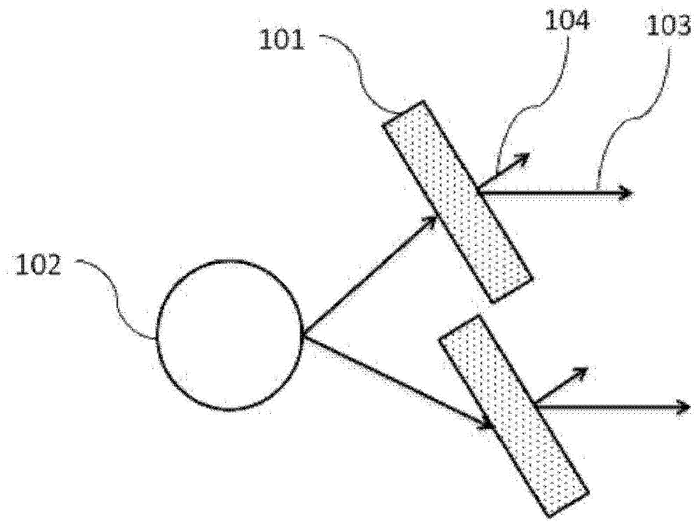
[0155] figure 1 A first embodiment of a device according to the invention that emits light in response to excitation of an activation element is shown. In the following, we denote anisotropic colloidal semiconductor nanocrystals with flat nanocrystals, whose smallest dimension and thickness are at least 1.5 times smaller than the other two. By flakes we mean flat nanocrystals that have at least one nanoscale dimension, ie thickness, and a lateral dimension that is larger than the thickness, typically 5 times the thickness. What we call the normal of a flat nanocrystal means the normal of the largest plane of the nanocrystal.

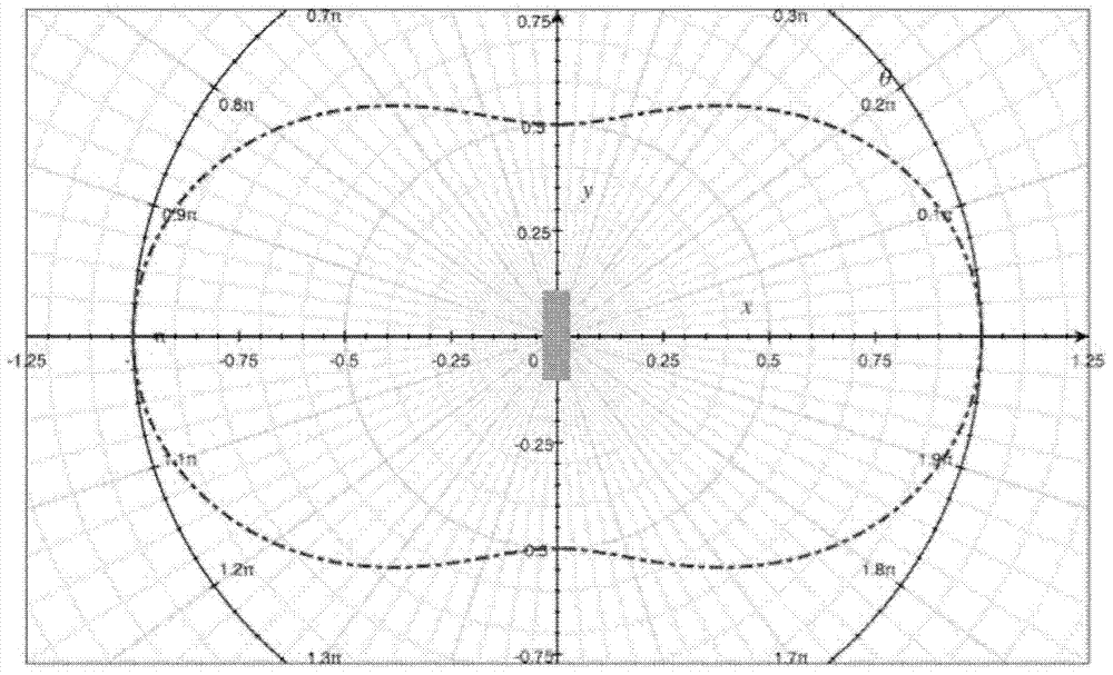
[0156] The device comprises at least one flat nanocrystal 101 and its actuating element 102 . The intensity and polarization of the light emitted by the device varies with the angle formed by the light emission direction 103 and the normal 104 to the larger plane of the nanocrystal.

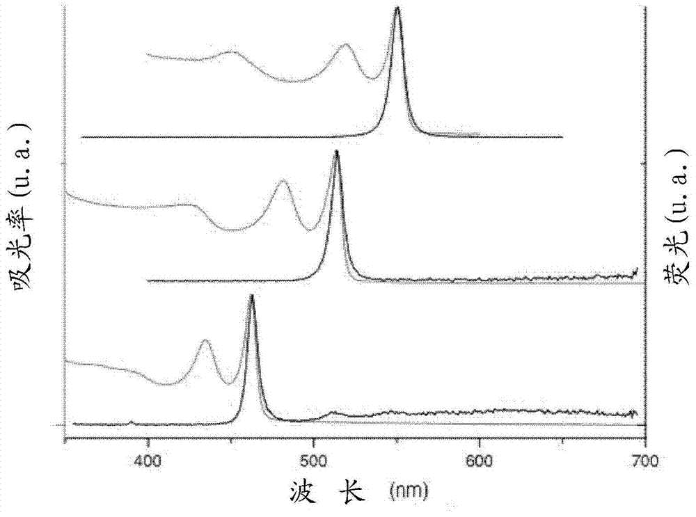
[0157] Flat nanocrystals are fluorophores whose emission wavelength...


PUM


Abstract

A device that emits light in response to an electrical or optical excitation, such as LEDs, displays, e-readers, device includes at least one anisotropic flat colloidal semiconductor nanocrystal whose smallest dimension, namely the thickness, is smaller than the other two by a factor of at least 1.5, the emitted light having an intensity and a polarization that vary according to the angle formed by the light emitting direction and the normal to the largest surface of the flat nanocrystal. The device allows to realize a light-emitting device exhibiting simultaneously a high emission spectral finesse and allows proper control of the wavelength, the directivity and/or polarization of the emitted light, and thus increases the brightness and color gamut of displays composed of such a device. Such devices are found for example in displays, televisions, mobile phones, tablets, or computers. The various embodiments of these devices are also presented.

Description

technical field [0001] The present invention relates to devices that emit light in response to electrical or optical excitation, such as light emitting diodes, displays, electronic readers, and the like. Such devices are found in eg monitors, televisions, mobile phones, tablets or computers. Although this type of device has been steadily developed, it still has problems in that it is limited in terms of color rendering, contrast, brightness, energy efficiency, and visual impression depending on the viewing angle. Background technique [0002] In order to completely restore the color, it is generally achieved by adding and synthesizing at least three complementary colors, especially red, green and blue. In the chromaticity diagram, the subset of available colors obtained by mixing different proportions of the three colors red, green, and blue is formed by the triangular relationship formed by the three coordinates associated with these three colors. This subset constitutes ...

Claims


Application Information

Patent Timeline
Patent Type & Authority Applications(China)
IPC IPC(8): B82Y30/00H05B33/14H01L33/06H01L33/50F21V9/40
CPCC09K11/883F21V9/10F21V9/16G02F1/133603H01L33/504H01L33/502C09K11/565H05B33/145C09K11/02B82Y20/00Y10S977/834H01L2933/0041F21K2/00Y10S977/773B82Y30/00Y10S977/95F21V9/30F21V9/40
Inventor 贝努瓦·马勒托马斯·庞斯埃尔莎·卡塞特
Owner NEXDOT
Why Eureka
Try Eureka