Engineered structure for high brightness solid-state light emitters

a technology of solid-state light emitters and engineered structures, which is applied in the direction of solid-state devices, electric lighting sources, and light sources with electric components, etc., can solve the problems of reducing efficiency, reducing light emission, and reducing efficiency, so as to improve luminous efficacy and brightness.

Active Publication Date: 2010-02-11
KIRSTEEN MGMT GRP
View PDF19 Cites 19 Cited by
  • Summary
  • Abstract
  • Description
  • Claims
  • Application Information

AI Technical Summary

Benefits of technology

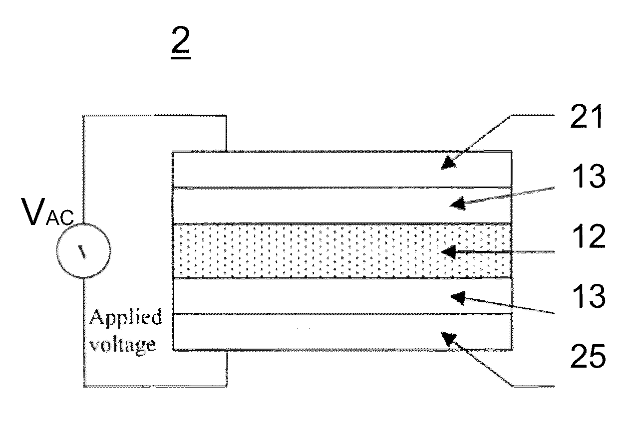
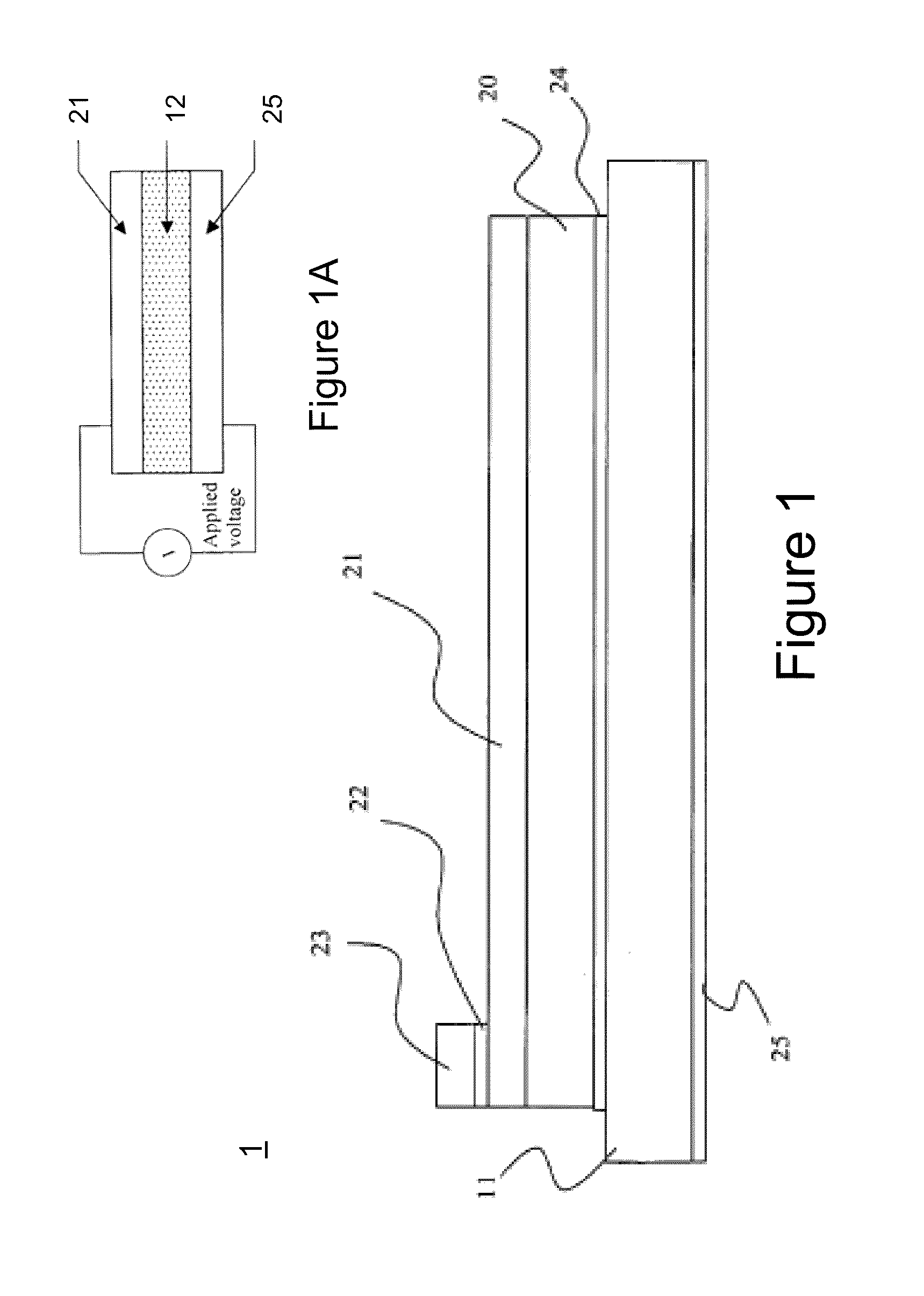
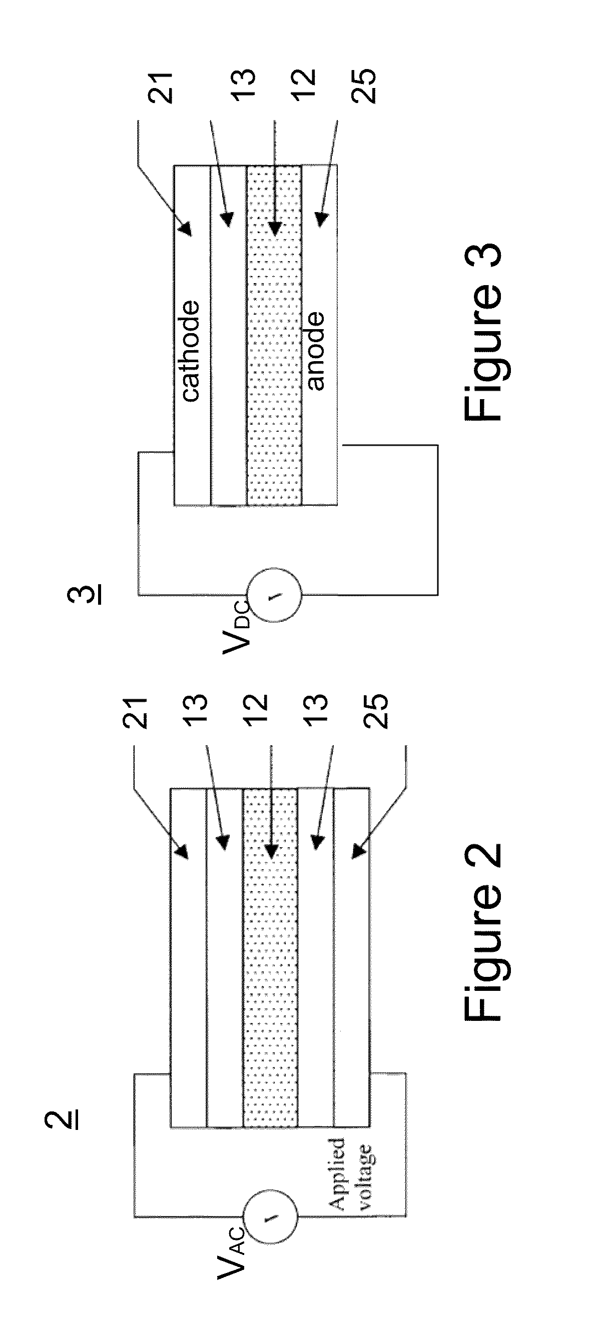
[0023]Advantageously, each drift layer has thickness relative to the electric field dependent on the respective excitation energy of an adjacent active layer, for controlling electron energy gain from the electric field for exciting light emission at the characteristic wavelength, and preferably the thickness is substantially equal to the required excitation energy divided by the electric field. Electrons traversing the drift layer gain energy from the electric field for excitation of the luminescent centers in an adjacent active layer at the respective excitation energy. In the ballistic regime, electrons gain energy e in the drift layers (in eV) equal to the electric field E (V / nm) multiplied by the thickness of the drift layer d. (nm). Preferably, each drift layer has a thickness that provides improved energy matching or tuning of the respective excitation energy for an adjacent active layer, thereby improving excitation efficiency and luminous efficacy.
[0025]The corresponding drift layers may comprise silicon dioxide or silicon nitride, although silicon dioxide is preferred. In another embodiment the host matrix material in active layers comprises aluminum oxide, and the drift layer dielectric comprise silicon dioxide, aluminum oxide, or aluminum doped silicon dioxide. Aluminum containing dielectrics, e.g. aluminum oxide, or SiAlON, may reduce clustering of rare earths, and allow high concentrations of luminescent centres to be incorporated before concentration quenching is observed. An aluminum oxide based structure is also believed to provide advantages for some applications because of the lower bandgap and conduction band offset or higher dielectric constant, and higher thermal conductivity relative to silicon dioxide are beneficial.
[0032]In some structures the composition of the dielectric host matrix is selected to shift the emission wavelength in each of a plurality of active layer dependent on the host material composition. For example, a layer stack comprising a plurality of active layers may comprises active layers each doped with a first rare earth species having an emission wavelength dependent on the composition of the dielectric SiaAlbOcNd, and successive active layers have different composition (i.e. values of a, b, c, and d are varied) to provide emission at a plurality of wavelengths. Such a structure is beneficial where improved control of the emission spectrum and wavelength over a narrow or broad range is required. Varying the composition of the host matrix material in different layers of the stack may provide for spectral tuning, for example, when it is desirable to use a limited number of rare earth dopants, a limited number of layers, or to provide for extended range of spectral tuning with one or multiple rare earth dopants.
[0038]Engineered emitter layer structures according to embodiments of the invention provide significant improvements in luminous efficacy and brightness over bulk structures comprising nanocrystals and / or rare earth luminescent centers, and conventional thin film electroluminescent devices.

Problems solved by technology

If the energy of incident electrons is too low there will be no light emission possible.
On the other hand, if the electrons possess too much energy there will be light emission but excess energy will be carried away in the form of heat, which reduces efficiency.
Furthermore, hot electrons can be responsible for damage to the host matrix, result in charging, and ultimately contribute to breakdown and failure of the device under bias.
Unfortunately, existing approaches to developing such silicon nano-particle materials have only been successful at producing very low concentrations of the rare earth element, which are not sufficient for many practical applications.
The reduced nano-particle excitation energy affects the efficiency of energy transfer from conducting electrons when these structures are electrically powered, thereby limiting the efficiency of light generation from such films.
In practice, however, careful control of deposition parameters, layer thickness, and thermal treatments is needed to control the size, uniformity and passivation of nanocrystal layers to obtain a desired emission wavelength and excitation energy, otherwise significant emission may be observed from lower energy interfacial states, resulting in loss of efficiency.
Thus, problems with known device structures and processes based on luminescent centres comprising rare earths and / or nanocrystals include inconsistent size, quality and uniformity of nanocrystals to obtain a desired wavelength of emission or excitation energy; quenching of emission from rare earth luminescent species at higher concentrations, and poor efficiency of excitation of luminescent centres either directly or by energy transfer from nano-particles to rare earth luminescent centres.
In particular, energy mismatches lead to poor excitation efficiency, i.e. if the excitation energy is too low, luminescent centers are not effectively excited, and if the excitation energy is too high, then energy is wasted in the excitation process.

Method used


Image

  • Engineered structure for high brightness solid-state light emitters
  • Engineered structure for high brightness solid-state light emitters
  • Engineered structure for high brightness solid-state light emitters

Examples


example 1

Rare Earth Doped Alumina

[0098]When the host matrix material in which rare earth luminescent species are embedded is aluminum oxide (alumina, Al2O3) rather than silicon dioxide, a number of advantages ensue:[0099]Since alumina is also an oxide, rare earths will be bound to oxygen, so as to be in the correct chemical state to emit light, e.g. as a trivalent state, such as Ce3+.[0100]The microstructure of alumina is such that octahedral cells are formed in which the rare earths can reside, with reduced clustering (C. E. Chryssou, et al, IEEE J. Quantum Electron. 34, 282 (1988)). Because they are strongly bound in these cells, they are unlikely to diffuse through the material, even at elevated temperatures, and therefore they are unlikely to cluster together. Clustering of two of more rare earths together changes their electronic or bonding configuration, so that they are no longer light emitters. The use of alumina helps to avoid this situation, allowing higher concentrations of rare e...

example 2

Rare Earth and Aluminum Co-doped in Silicon Dioxide

[0108]Another material which provides a suitable host matrix material for the active material comprises aluminum doped silicon dioxide. Co-doping of rare earth luminescent species and aluminum into silicon dioxide provides advantages over rare earth doped silicon dioxide host material without aluminum doping by reducing clustering effects. Consequently it may be possible to dope layers with more than the 1 to 5% of rare earth dopants typically used, before clustering effects are observed. Not only does the aluminum doping inhibit clustering effects, when used with certain rare earth dopants, notably cerium, where the bandgap of the host affects the shape of the luminescence spectra, it has been observed that the emission wavelength of the active layer may be shifted in proportion to the amount of aluminum doping. Therefore appropriate selection of rare earth luminescent species and aluminum doping concentration provides for more con...

example 3

Rare Earth Doped Silicon Oxynitrides of the General Structure SiaObNc

[0116]As described with respect to Examples 1 and 2 above, a multilayer structure may be provided comprising a plurality of active layers each comprising a rare earth doped host matrix material of a dielectric material selected to control clustering effects, allowing higher concentrations of rare earth species to be incorporated for higher brightness, and possibly improved efficiency, and / or for colour control. Thus in this example, each active layer comprises a dielectric of the general formula SiaObNc in varying ratios, i.e. nitrogen containing oxides or silicon oxynitrides. The drift layers preferably comprise an appropriate thickness of silicon dioxide, as described above.

[0117]In these examples, addition of nitrogen to the rare earth doped layers provides a red shift in the emission spectrum of the rare earth luminescent species, e.g. cerium, and by adding judicious amounts of nitrogen the desired wavelength ...


PUM


Abstract

Electroluminescent (EL) light emitting structures comprises one or more active layers comprising rare earth luminescent centres in a host matrix for emitting light of a particular colour or wavelength and electrodes for application of an electric field and current injection for excitation of light emission. The host matrix is preferably a dielectric containing the rare earth luminescent centres, e.g. rare earth doped silicon dioxide, silicon nitride, silicon oxynitrides, alumina, dielectrics of the general formula SiaAlbOcNd, or rare earth oxides. For efficient impact excitation, corresponding drift layers adjacent each active layer have a thickness related to a respective excitation energy of an adjacent active layer. A stack of active layers emitting different colours may be combined to provide white light. For rare earth species having a host dependent emission spectrum, spectral emission of the stack may be tuned by appropriate selection of a different host matrix in successive active layers.

Description

CROSS-REFERENCE TO RELATED APPLICATIONS[0001]This application is a continuation-in-part of U.S. patent application Ser. No. 11 / 642,788 filed Dec. 12, 2006, entitled “Engineered structure for solid state light emitters” claiming priority from U.S. Provisional patent application No. 60 / 754,185 filed Dec. 28, 2005 and No. 60 / 786,730 filed Mar. 29, 2006; this application is also a continuation-in-part of U.S. patent application Ser. No. 12 / 015,285 filed Jan. 16, 2008 entitled “Pixel structure for a solid state light emitting device” which is a continuation in part of U.S. patent applications Ser. No. 11 / 642,813 filed Dec. 21, 2006, claiming priority from U.S. Provisional patent application No. 60 / 754,185 Dec. 28, 2005; this application also claims priority from U.S. provisional application No. 61 / 083,751 filed Jul. 25, 2008 entitled “Solid state light emitters using rare earths and aluminum”; all of these applications are incorporated herein by reference for all purposes.TECHNICAL FIELD...

Claims


Application Information

Patent Timeline
Patent Type & Authority Applications(United States)
IPC IPC(8): H01L33/00
CPCH05B33/22H05B33/145
Inventor CALDER, IAINMINER, CARLACHIK, GEORGEMACELWEE, THOMAS
Owner KIRSTEEN MGMT GRP
Why Eureka
Try Eureka