Infrared light-concentrating chip

A chip and infrared technology, applied in optics, nonlinear optics, instruments, etc., can solve the problems of spectrum separation without adjustable function, large volume, mass and inertia, poor spectrum adaptability, etc., and achieve infrared light energy utilization rate High, high control precision, easy to match the effect of coupling

Active Publication Date: 2015-02-04
HUAZHONG UNIV OF SCI & TECH
View PDF4 Cites 2 Cited by
  • Summary
  • Abstract
  • Description
  • Claims
  • Application Information

AI Technical Summary

Problems solved by technology

[0003] At present, through the circular symmetric concentric zone plate with a specific shape structure, the axial multi-focus discrete focusing and the spotlight spectrum space separation technology are performed on the incident infrared light wave, which presents several obvious defects, including: (1) Establishment based on a specific wavelength The special shape profile and structural size of the zone plate only perform multi-focus discrete beamforming operations for specific wavelengths. The weak changes in the spectrum will greatly reduce the performance of discrete beamforming or spectrum space separation, and the spectrum adaptability is poor; (2) The axis of the light wave Focused multi-focus construction or spectrum separation does not have adjustable functions, and the focal length and point spread function cannot be adjusted. The adaptability of the target and the working environment and electrical environment is poor; (3) focus or point spread adjustment The function is usually based on the mechanical movement between the zone plate and the auxiliary lens. The volume, mass and inertia of the actuator are large, and it needs to be equipped with a complicated drive and control device. The response is slow, the state transition time is long, and the infrared optical state cannot be performed due to mechanical movement. (4) Only the axial spectrum separation operation with large wavelength difference can be performed

Method used


Image

  • Infrared light-concentrating chip
  • Infrared light-concentrating chip
  • Infrared light-concentrating chip

Examples


Embodiment Construction

[0021] In order to make the object, technical solution and advantages of the present invention clearer, the present invention will be further described in detail below in conjunction with the accompanying drawings and embodiments. It should be understood that the specific embodiments described here are only used to explain the present invention, not to limit the present invention. In addition, the technical features involved in the various embodiments of the present invention described below can be combined with each other as long as they do not constitute a conflict with each other.

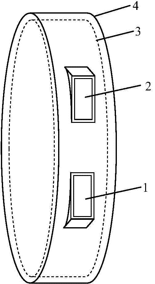
[0022] Such as figure 1 As shown, the infrared concentrating chip of the embodiment of the present invention includes a chip housing 4 and a cylindrical liquid crystal phase modulation structure 3 . The liquid crystal phase modulation structure 3 is packaged in the chip case 4 and fixedly connected with the chip case 4 , and its light incident surface and light exit surface are exposed through ...


PUM


Abstract

The invention discloses an infrared light-concentrating chip. The chip comprises a cylindrical liquid crystal phase modulation framework; the cylindrical liquid crystal phase modulation framework comprises a liquid crystal material layer, and a first liquid crystal initial orientation layer, a first electric isolation layer, a patterned electrode layer, a first substrate and a first infrared antireflection film which are sequentially arranged on the upper surface of the liquid crystal material layer, and a second liquid crystal initial orientation layer, a second electric isolation layer, a public electrode layer, a second substrate and a second infrared anti-reflection film which are sequentially arranged on the lower surface of the liquid crystal material layer; the patterned electrode layer is composed of a circular conductive film, and at least one circular-circle-shaped conductive film concentrically arranged on the periphery of the circular conductive film; the diameter of the circular conductive film is greater than the radial width of the adjacent circular-circle-shaped conductive film; when a plurality of circular-circle-shaped conductive films are arranged, the plurality of circular-circle-shaped conductive films are sequentially arranged on the periphery of the circular conductive film, and the radial width of each circular-circle-shaped conductive film is progressively decreased. The infrared light-concentrating chip has high focusing efficiency on infrared wave beams and good optical field adaptability and is small in size, light in weight and easy to couple with other optical and photoelectric mechanical structures.

Description

technical field [0001] The invention belongs to the technical field of infrared light wave precision measurement and control, and more specifically relates to an infrared concentrating chip. Background technique [0002] So far, the technology of performing multi-focus discrete beamforming in the direction of the optical axis for infrared incident light waves through a circularly symmetrical concentric zone plate with a specific morphology has achieved performance improvement and functional expansion of conventional optical structures or systems. Construct a beamforming processing and transformation architecture based on ultra-thin chip and light wave coherent enhancement, develop light energy utilization efficiency diffraction enhancement, and perform spectral beamforming spectrum space separation of polychromatic light waves based on specific spatial arrangement of diffraction phase structure, etc. aspect, it has been widely used. With the continuous and rapid development...

Claims


Application Information

Patent Timeline
Patent Type & Authority Applications(China)
IPC IPC(8): G02F1/1343G02F1/133G02F1/29G01J3/12
CPCG01J3/12G02F1/1313G02F1/1343
Inventor 张新宇雷宇佟庆罗俊桑红石谢长生
Owner HUAZHONG UNIV OF SCI & TECH
Why Eureka
Try Eureka