Array substrate, display panel and display device

An array substrate and board surface technology, which is applied in the field of display panels, display devices, and array substrates, and can solve the problem that signal traces around the display area occupy additional non-display areas, etc.

Inactive Publication Date: 2015-02-18
CHONGQING BOE OPTOELECTRONICS +1
View PDF7 Cites 31 Cited by
  • Summary
  • Abstract
  • Description
  • Claims
  • Application Information

AI Technical Summary

Problems solved by technology

[0005] In view of this, in order to solve the problems in the prior art, embodiments of the present invention provide an array substrate, a display panel and a display device, which can solve the problem in the prior art that the signal traces around the display area need to occupy additional non-display areas on both sides , so that when the array substrate is applied to a display panel, the borders on both sides of the display area of ​​the display panel can be simplified

Method used


Image

  • Array substrate, display panel and display device
  • Array substrate, display panel and display device
  • Array substrate, display panel and display device

Examples


Embodiment Construction

[0034] The following will clearly and completely describe the technical solutions in the embodiments of the present invention with reference to the accompanying drawings in the embodiments of the present invention. Obviously, the described embodiments are only some, not all, embodiments of the present invention. Based on the embodiments of the present invention, all other embodiments obtained by persons of ordinary skill in the art without making creative efforts belong to the protection scope of the present invention.

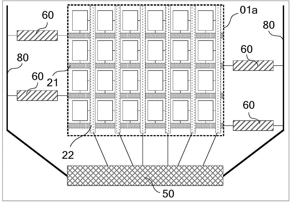
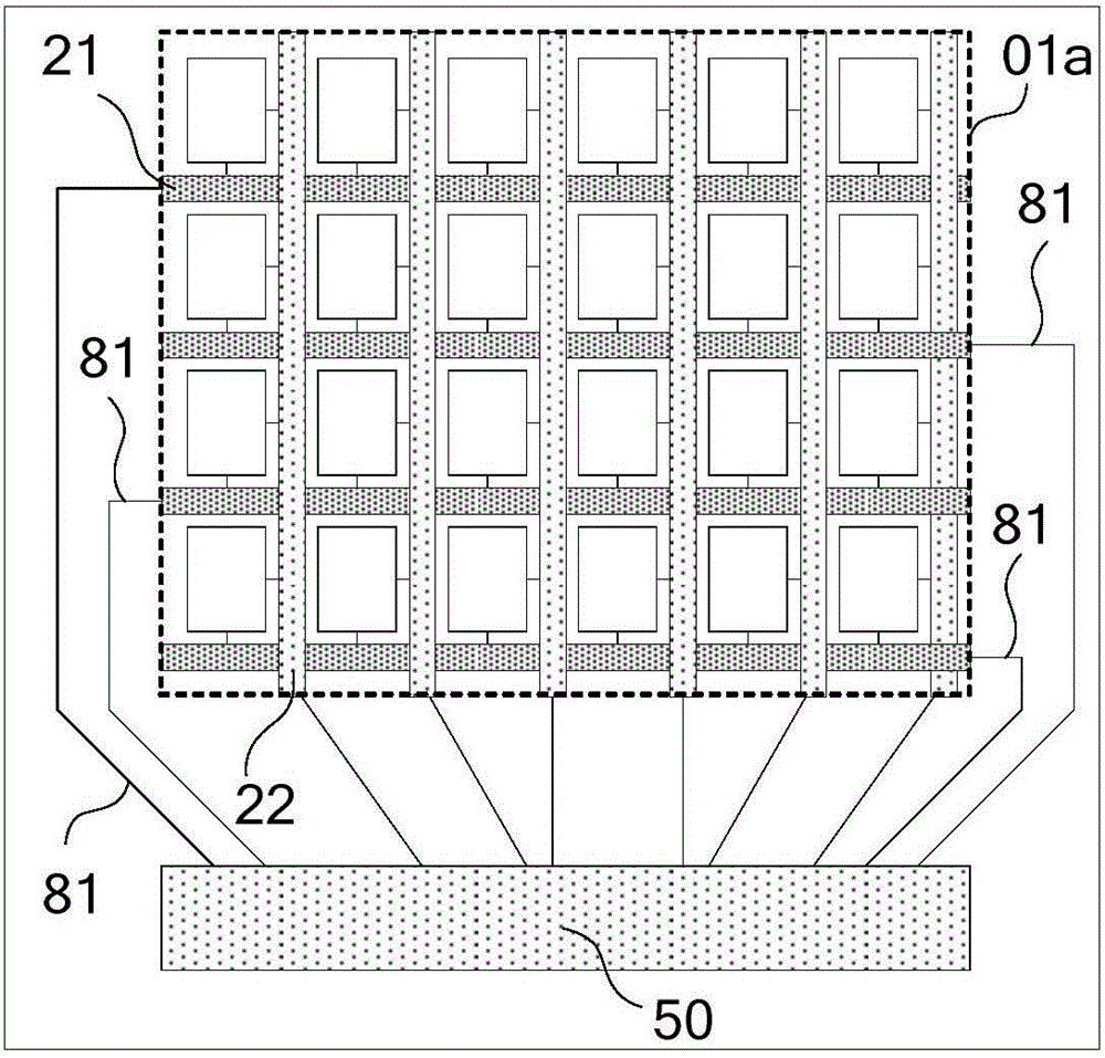
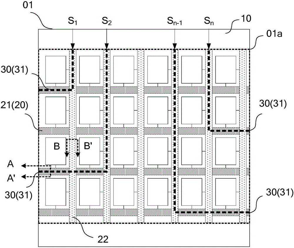
[0035] An embodiment of the present invention provides an array substrate 01, such as figure 2 As shown, the array substrate 01 includes a base substrate 10, and a signal line 20 located on the base substrate 10 corresponding to the display area 01a of the array substrate 01; the array substrate 01 also includes: The signal wire 30 between the pattern layer of the signal wire 20 and the substrate 10 ; the signal wire 30 is used to input signals to the signal ...


PUM


Abstract

The embodiment of the invention provides an array substrate, a display panel and a display device and relates to the technical field of displaying. The problem that a peripheral signal routing in a display region needs to occupy extra non-display regions on two sides in the prior art can be solved; therefore, when the array substrate is applied to the display panel, borders on two sides of the display region of the display panel can be simplified. The array substrate comprises a bottom substrate and a signal line which is positioned on the bottom substrate and corresponds to the display region of the array substrate, and the array substrate further comprises a signal line wire positioned between a pattern layer of the signal line and the bottom substrate; the signal line wire is used for inputting a signal to the signal line. The invention also provides preparation of the array substrate and the display panel comprising the array substrate.

Description

technical field [0001] The present invention relates to the field of display technology, in particular to an array substrate, a display panel and a display device. Background technique [0002] In the array substrate provided by the prior art, the grid lines and data lines arranged vertically and vertically define a plurality of pixel units in the array substrate, and these pixel units constitute the display area in the array substrate; In the display area, the array substrate also includes a driving integrated circuit IC unit for inputting signals to the gate line and the data line. [0003] Among them, such as Figure 1A As shown, for a new type of array substrate with a GOA unit (Gate Driver on Array, array substrate row drive), the GOA unit 60 and the gate scanning circuit signal line 80 for connecting the GOA unit and the IC unit 50 need to be arranged in the display area 01a In the non-display area on both sides; such as Figure 1B As shown, for a conventional array ...

Claims


Application Information

Patent Timeline
Patent Type & Authority Applications(China)
IPC IPC(8): G02F1/1362H01L27/12
CPCG02F1/136286H01L27/124H01L2924/0002H10K59/131H10K2102/3026H01L2924/00H01L25/167
Inventor 汪锐尚飞王武李少茹
Owner CHONGQING BOE OPTOELECTRONICS
Why Eureka
Try Eureka