Check patentability & draft patents in minutes with Patsnap Eureka AI!

NOR-type flash memory structure and preparation method thereof

A manufacturing method and flash memory technology, applied in semiconductor/solid-state device manufacturing, electrical components, electrical solid-state devices, etc., can solve the problems of low efficiency, long erasing time, large RC delay, etc., achieve small RC delay and improve device performance , Improve the effect of erasing efficiency

Inactive Publication Date: 2015-02-18
SHANGHAI HUAHONG GRACE SEMICON MFG CORP
View PDF3 Cites 3 Cited by
  • Summary
  • Abstract
  • Description
  • Claims
  • Application Information

AI Technical Summary

Problems solved by technology

[0002] In the existing flash memory structure, since the floating gate has no tip, the erasing time is long and the efficiency is low
And because there is no silicide in the control gate in the existing flash memory structure, the RC delay is relatively large

Method used


Image

  • NOR-type flash memory structure and preparation method thereof
  • NOR-type flash memory structure and preparation method thereof
  • NOR-type flash memory structure and preparation method thereof

Examples


Embodiment Construction

[0012] In order to make the content of the present invention clearer and easier to understand, the content of the present invention will be described in detail below in conjunction with specific embodiments and accompanying drawings.

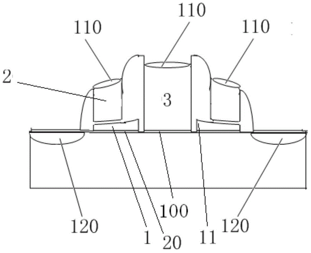
[0013] figure 1 A NOR flash memory structure according to a preferred embodiment of the present invention is schematically shown.

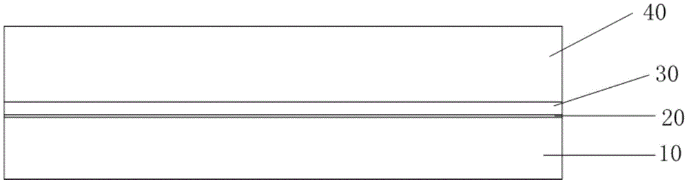
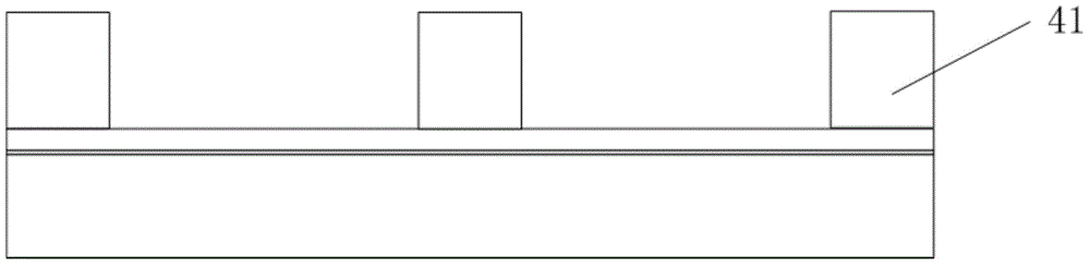
[0014] Such as figure 1 As shown, the NOR flash memory structure according to the preferred embodiment of the present invention includes: a silicon dioxide layer 20 disposed on a substrate and a gate structure disposed on the silicon dioxide layer 20 .

[0015] Wherein, the gate structure includes two stacked gate structures arranged on both sides of the word line structure 3 and separated from the word line structure 3 by silicon dioxide. Furthermore, each stacked gate structure includes a floating gate 1 and a control gate 2 separated by silicon dioxide from bottom to top, wherein the upper surface of the floati...


PUM


Abstract

The invention provides an NOR-type flash memory structure and a preparation method of the NOR-type flash memory structure. The NOR-type flash memory structure comprises a silicon dioxide layer arranged on a substrate and a gate structure arranged on the silicon dioxide layer, wherein the gate structure comprises two stacked gate structures, and the two stacked gate structures are arranged on the two sides of a word line structure respectively and isolated from the word line structure through silicon dioxide; each stacked gate structure comprises a floating gate and a control gate which are isolated from bottom to top through silicon dioxide, and the upper surface of the floating gate gradually turns up in the direction close to the word line structure; silicide is arranged on the control gates and the word line structure; bit lines are formed in the surface of the substrate and located on the two sides of the gate structure.

Description

technical field [0001] The invention relates to the field of semiconductor manufacturing, and more specifically, the invention relates to a NOR flash memory structure and a manufacturing method thereof. Background technique [0002] In the existing flash memory structure, since the floating gate has no tip, the erasing time is long and the efficiency is low. Moreover, since the control gate in the existing flash memory structure does not have silicide, the RC delay is relatively large. Thus, it is desirable to improve the performance of flash memory structures. Contents of the invention [0003] The technical problem to be solved by the present invention is to provide a NOR flash memory structure and a manufacturing method thereof that can speed up erasing time and reduce RC delay in view of the above-mentioned defects in the prior art. [0004] In order to achieve the above technical purpose, according to the first aspect of the present invention, a NOR flash memory str...

Claims


Application Information

Patent Timeline
IPC IPC(8): H01L27/115H01L21/8247
Inventor 于涛
Owner SHANGHAI HUAHONG GRACE SEMICON MFG CORP
Features
  • R&D
  • Intellectual Property
  • Life Sciences
  • Materials
  • Tech Scout
  • Unparalleled Data Quality
  • Higher Quality Content
  • 60% Fewer Hallucinations
Learn More