
Applied to amoled pixel unit circuit with common anode

A common anode and pixel unit technology, applied in the field of pixel circuits, can solve the problems of difficult high-contrast adjustment and difficult to meet high-contrast performance requirements at the same time, and achieve high-contrast adjustment, high-performance requirements, and high-contrast effects

Active Publication Date: 2017-04-19
NANJING GUOZHAO OPTOELECTRONICS TECH CO LTD
View PDF7 Cites 0 Cited by
  • Summary
  • Abstract
  • Description
  • Claims
  • Application Information

AI Technical Summary

Problems solved by technology

However, the current pixel unit circuit is still insufficient in the contrast adjustment of AMOLED light emission, it is difficult to achieve high contrast adjustment, and it is difficult to meet the performance requirements of high contrast while obtaining high brightness

Method used


Image

  • Applied to amoled pixel unit circuit with common anode
  • Applied to amoled pixel unit circuit with common anode

Examples


Embodiment Construction

[0012] The present invention will be further described below in conjunction with accompanying drawing.

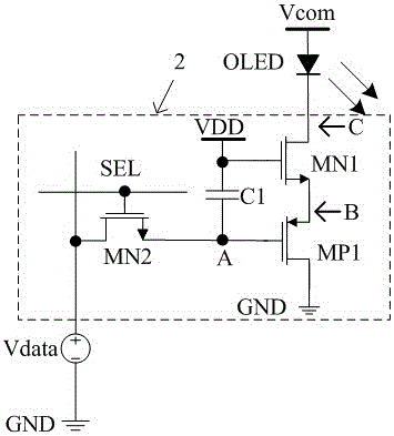
[0013] figure 1 It is a pixel circuit diagram of the present invention, which is composed of a specific pixel circuit in the dotted line frame 2, an external input voltage source Vdata (pixel input data voltage), and an external OLED. The drain of the N-type MOS transistor MN2 is connected to the positive terminal of the input voltage source Vdata, and the source of the N-type MOS transistor MN2 is connected to one end of the capacitor C1 and the gate of the P-type MOS transistor MP1. The gate of the N-type MOS transistor MN2 is connected to the row selection control signal SEL. The drain of the P-type MOS transistor MP1 and the negative end of the voltage source Vdata are connected to the ground GND. The source of the P-type MOS transistor MP1 is connected to the source of the N-type MOS transistor MN1. The gate of the N-type MOS transistor MN1 and the other end of the ...


PUM


Abstract

The invention discloses a pixel unit circuit applied to an AMOLED with a common anode. The pixel unit circuit comprises a regulating tube MN1, a driving tube MP1, a switching tube MN1 and a storage capacitor C1. The drain electrode of the switching tube MN2 is connected with the positive end of an input voltage source Vdata. The source electrode of the switching tube MN2 is connected with one end of the storage capacitor C1 and the gate electrode of the driving tube MP1. The gate electrode of the switching tube MN2 is connected with a row selection control signal SEL. The drain electrode of the driving tube MP1 and the negative end of the input voltage source Vdata are connected with the ground GND. The source electrode of the driving tube MP1 is connected with the source electrode of the regulating tube MN1. The gate electrode of the regulating tube MN1 and the other end of the storage capacitor C1 are connected with a power supply VDD. The drain electrode of the regulating tube MN1 is connected with the cathode of the OLED. The maximum brightness of the OLED is enabled to be unchanged, and the minimum current is enabled to be lowered in the dark state so that luminescence contrast ratio of the OLED is increased.

Description

technical field [0001] The invention belongs to the field of microelectronics and display technology, and in particular relates to a pixel circuit applied to an AMOLED drive chip. Background technique [0002] As a new generation of display technology, active organic light emitting diode (AMOLED) has the advantages of active light emission, wide viewing angle, low driving voltage, high luminous efficiency, fast response speed, low power consumption, wide range of operating temperature adaptability, light and thin volume, and can realize flexible display And other characteristics, has very broad prospects. It can be used in mobile terminal displays, involving various industries and fields such as scientific research, entertainment, communication, military affairs, and medical treatment, and its potential is very huge. In addition to studying OLED devices with high stability, it is also important to study their driving technology. [0003] According to different driving meth...

Claims


Application Information

Patent Timeline
Patent Type & Authority Patents(China)
IPC IPC(8): G09G3/3225H01L27/32G09G3/3233
Inventor 杨淼张白雪任健雄曹允
Owner NANJING GUOZHAO OPTOELECTRONICS TECH CO LTD
Learn More