Pixel circuit for silicon-based AMOLED driving chip

A technology for driving chips and pixel circuits, applied in instruments, static indicators, etc., can solve the problems of difficulty in high brightness and high contrast, small adjustable range, complex structure, etc., and achieve area saving, large adjustable range, and simple structure. Effect

Inactive Publication Date: 2015-03-04
NO 55 INST CHINA ELECTRONIC SCI & TECHNOLOGYGROUP CO LTD
View PDF6 Cites 27 Cited by
  • Summary
  • Abstract
  • Description
  • Claims
  • Application Information

AI Technical Summary

Problems solved by technology

Today's existing pixel circuits are not effective in achieving high contrast adjustment, the adjustable range is small, the structure is complex, and it is difficult to achieve high brightness and high contrast at the same time

Method used


Image

  • Pixel circuit for silicon-based AMOLED driving chip
  • Pixel circuit for silicon-based AMOLED driving chip
  • Pixel circuit for silicon-based AMOLED driving chip

Examples


Embodiment Construction

[0020] The present invention will be further described below in conjunction with accompanying drawing.

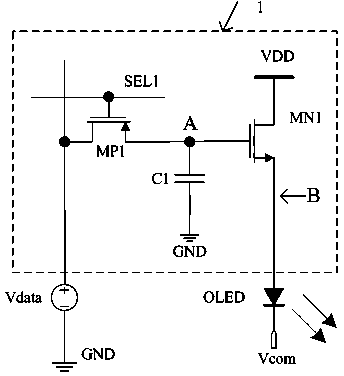
[0021] figure 1 Shown is an existing pixel circuit diagram, which is composed of a specific pixel circuit 1 in a dotted line frame, an external input voltage source Vdata, and an external OLED. The drain of the P-type MOS transistor MP1 is connected to the positive terminal of the input voltage source Vdata, and the source of the P-type MOS transistor MP1 is connected to one end of the capacitor C1 and the gate of the N-type MOS transistor MN1. The gate of the P-type MOS transistor MP1 is connected to the row selection control signal SEL1. The negative end of the voltage source Vdata and the other end of the capacitor C1 are connected to the ground GND. The drain of the N-type MOS transistor MN1 is connected to the voltage VDD, and the source of the N-type MOS transistor MN1 is connected to the anode of the OLED. The cathode of the OLED is connected to the Vcom voltage. ...


PUM


Abstract

The invention discloses a pixel circuit for a silicon-based AMOLED driving chip, which comprises a driving tube MN2, a switching tube MP2, a voltage controlled resistor and a storage capacitor C2. Resistance of the voltage controlled resistor is increased along with decreasing of pixel data voltage Vdata, OLED anode voltage in a dark state is reduced, pixel output current becomes small, and thus the minimal brightness is lower; resistance of the voltage controlled resistor is decreased to be ignored along with increasing of pixel data voltage Vdata, the OLED anode voltage is increased due to increasing of the pixel data voltage, and the maximal brightness remains unchanged. Compared with the prior pixel circuit, contrast of OLED light emitting can be significantly increased. Particularly, when common cathode voltage Vcom needs to be adjusted to acquire high current output in order to acquire high brightness, the circuit does not significantly increase the minimal current outputted by the pixel, and thus, high contrast of the OLED in a high brightness state can be realized.

Description

technical field [0001] The invention belongs to the field of microelectronics and display technology, in particular to a high-contrast pixel circuit applied to a silicon-based AMOLED micro-display driver chip. Background technique [0002] Silicon-based active organic light-emitting diode (AMOLED) microdisplay is a branch of display technology, which realizes the combination of OLED technology and silicon-based integrated circuit technology. Silicon-based AMOLED microdisplay has the characteristics of thinness and lightness, active light emission, wide viewing angle, no flicker and jitter, low-voltage drive, high luminous efficiency, fast response speed, low power consumption, and high integration. It can be used in various display fields. Because of its small size, it has great advantages in portable display applications. At present, it is mainly used in helmet-mounted displays, glasses-type displays, etc., and can also be used in other mobile terminal displays, involving ...

Claims


Application Information

Patent Timeline
Patent Type & Authority Applications(China)
IPC IPC(8): G09G3/32G09G3/3258
Inventor 杨淼张白雪任健雄曹允
Owner NO 55 INST CHINA ELECTRONIC SCI & TECHNOLOGYGROUP CO LTD
Why Eureka
Try Eureka