
3D Quantum Cellular Automata Adder

A technology of quantum cells and automata, applied in instruments, electrical digital data processing, digital data processing components, etc., can solve the problems of high power consumption and large area, and achieve the effect of low power consumption and less hardware resources

Inactive Publication Date: 2017-05-17
NANJING UNIV OF AERONAUTICS & ASTRONAUTICS
View PDF2 Cites 0 Cited by
  • Summary
  • Abstract
  • Description
  • Claims
  • Application Information

AI Technical Summary

Problems solved by technology

[0004] At present, the existing two-dimensional quantum cellular automata adder has a large area, so it uses more hardware resources and consumes more power.

Method used


Image

  • 3D Quantum Cellular Automata Adder
  • 3D Quantum Cellular Automata Adder
  • 3D Quantum Cellular Automata Adder

Examples


Embodiment Construction

[0044] Below in conjunction with accompanying drawing, technical scheme of the present invention is described in further detail:

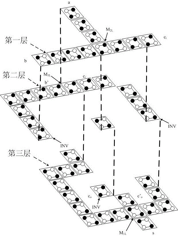
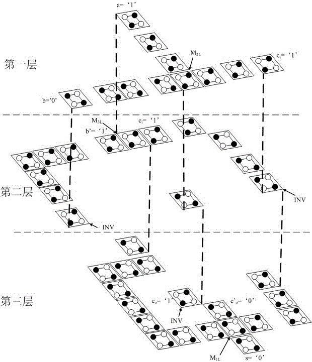
[0045] Such as figure 1 and figure 2 As shown, the present invention discloses a three-dimensional quantum cellular automata adder, including seven quantum cellular automata connections, a two-dimensional majority logic gate, a two-layer three-dimensional majority logic gate, a three-layer three-dimensional multiple logic gates, first to fourth three-dimensional inverters, a first two-dimensional inverter and a second two-dimensional inverter;

[0046] The three-dimensional quantum cellular automaton adder is distributed on three circuit layers and has three input terminals and two output terminals;

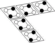
[0047]The two-layer three-dimensional majority logic gate includes five cells, four of which are located in the upper circuit and are T-shaped, and the other cell is located in the middle circuit and is directly below the junction of the upper T-sh...


PUM


Abstract

The invention discloses a three-dimensional quantum cellular automata adder, which comprises seven quantum cellular automata connecting lines, a two-dimensional majority logic gate, a two-layer three-dimensional majority logic gate, a three-layer three--dimensional majority logic gate, a first three-dimensional phase inverter, a second three-dimensional phase inverter, a third three-dimensional phase inverter, a fourth three-dimensional phase inverter, a first two-dimensional phase inverter and a second two-dimensional phase inverter. Compared with a traditional two-dimensional quantum cellular automata adder, the three-dimensional quantum cellular automata adder provides an extra one-dimensional computation space, so that fewer cells are required, and meanwhile, the space and the power consumption of a circuit are drastically reduced. The three-dimensional quantum cellular automata adder is a novel quantum cellular automata adder which has the advantages of being low in three-dimensional power consumption and small in area.

Description

technical field [0001] The invention relates to the field of circuit design based on quantum cellular automata, in particular to a three-dimensional quantum cellular automata adder. Background technique [0002] Integrated circuits are undergoing a transition from the era of microelectronics to the era of nanoelectronics. As the feature size of complementary metal-oxide-semiconductor (CMOS) devices shrinks to less than 20 nanometers, CMOS technology will soon reach its physical limits. Since it is difficult for CMOS devices to solve the quantum effects caused by size reduction and the increasingly serious heat dissipation and power consumption problems, the development of integrated circuits based on CMOS technology will encounter bottlenecks, and these difficulties and problems are difficult to solve by improving existing processes and technology to solve it fundamentally. According to the International Semiconductor Technology Roadmap Report (ITRS), when the feature size...

Claims


Application Information

Patent Timeline
Patent Type & Authority Patents(China)
IPC IPC(8): G06F7/494
Inventor 刘伟强
Owner NANJING UNIV OF AERONAUTICS & ASTRONAUTICS
Learn More