High utilization photo-voltaic device

A photovoltaic and device technology, applied in the field of improved photovoltaic devices, can solve the problems of capturing photons and being unable to use them

Inactive Publication Date: 2015-03-11
DOW GLOBAL TECH LLC
View PDF13 Cites 2 Cited by
  • Summary
  • Abstract
  • Description
  • Claims
  • Application Information

AI Technical Summary

Problems solved by technology

As a result, some types of PV devices currently known cannot utilize a significant portion of the effective solar area to capture photons

Method used


Image

  • High utilization photo-voltaic device
  • High utilization photo-voltaic device
  • High utilization photo-voltaic device

Examples


Embodiment Construction

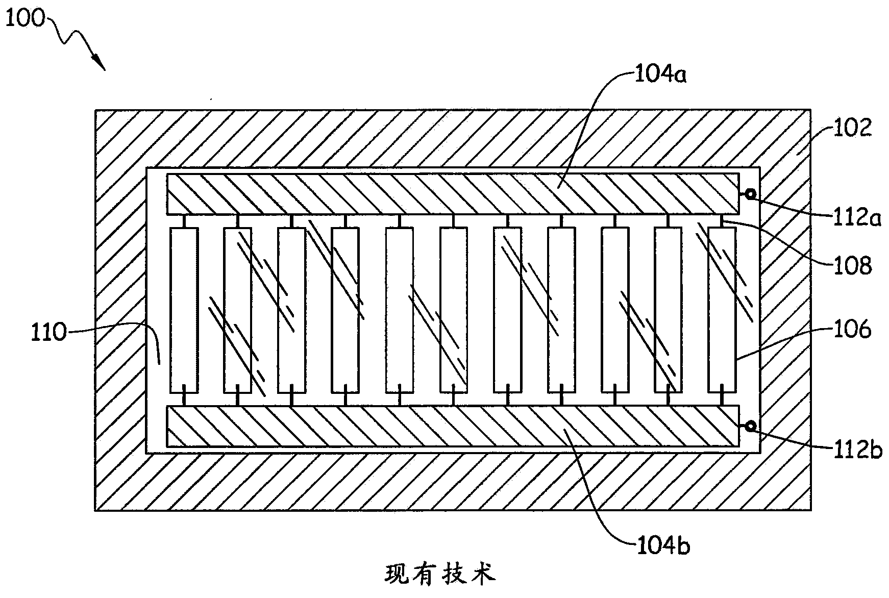
[0018] refer to figure 1 , schematically depicts a previously known PV device 100 . The PV device 100 in this example is a building-integrated cell, such as placed on a roof shingle or other building material unit. The PV device 100 includes a substrate 102, a plurality of photovoltaic (PV) cells 106, and electrical connections 108 to a first bus bar 104a and a second bus bar 104b. The PV device 100 also includes couplings 112a, 112b to external circuits. PV device 100 includes a transparent cover 110 , such as a glass cover, that allows light to reach PV cell 106 and provides protection to PV cell 106 . exist figure 1 As can be seen in , the spacing between the bus bars 104a, 104b and the PV cells 106 competes for space within the frame of the transparent cover 110, while for a given size and location of the PV device 100 and transparent cover 110 reduces the amount of radiation incident on the PV cells. amount of light.

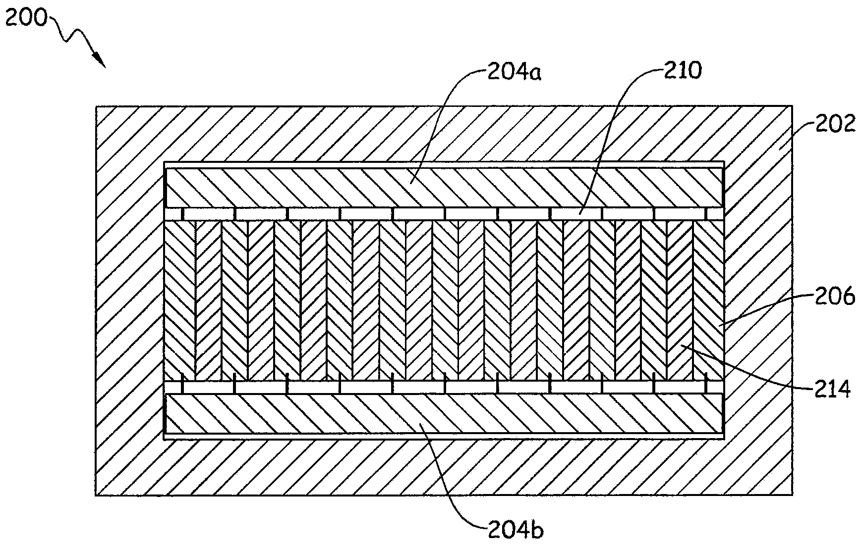
[0019] figure 2 is a schematic illustration of...


PUM


Abstract

An article of manufacture includes a first and second PV cell layer, where the first and second PV cell layers are at least partially displaced from each other and define a continuous optical coverage area throughout a solar active area. The article provides for enhanced utilization of the active solar area.

Description

technical field [0001] The present invention relates to improved photovoltaic devices, and more particularly but exclusively to photovoltaic devices with increased effective solar area utilization. Background technique [0002] Currently known photovoltaic (PV) devices include active solar area, which is the portion of the PV device that receives photons and converts them into usable electrical energy. In many devices, there is an unutilized portion of the active solar area that is reserved for electrically connecting assembly elements (such as bus bars and / or conductive elements that carry current within and between cells of a PV device) and / or is The area covered by the components of the electrical connection assembly. Certain PV materials require spacing around or between cells to prevent shunt current, provide heat transfer due to cell shape and size availability limitations, and / or for other reasons. Consequently, certain types of PV devices currently known cannot uti...

Claims


Application Information

Patent Timeline
Patent Type & Authority Applications(China)
IPC IPC(8): H01L31/02H01L31/05H01L31/043H02S20/25
CPCH02S20/25H01L2924/0002H01L31/02021H01L31/0504H01L31/043Y02E10/50Y02B10/12H02S20/00H01L2924/00Y02B10/10H01L31/0443H01L31/0201
Inventor 刘华冯捷L·C·洛佩斯R·K·费斯特K·L·考夫曼
Owner DOW GLOBAL TECH LLC
Why Eureka
Try Eureka