semiconductor structure

A semiconductor and carrier technology, applied in the field of semiconductor structures with anti-stress regions, can solve the problems of reducing the yield of semiconductor structures by 200%, lack of general products, inconvenience, etc.

Active Publication Date: 2017-09-15
CHIPBOND TECH
View PDF4 Cites 0 Cited by
  • Summary
  • Abstract
  • Description
  • Claims
  • Application Information

AI Technical Summary

Problems solved by technology

[0002] see Image 6 , is a conventionally known semiconductor structure 200, which has a carrier 210, a first protective layer 220, a second protective layer 230, and a third protective layer 240, because the first protective layer 220, the second protective layer 230 and the third protective layer 240 are quadrangular and the first protective layer 220, the second protective layer 230 and the third protective layer 240 are stacked on the carrier 210, so the stress of the semiconductor structure 200 is easy to concentrate on The overlapping corner of the first passivation layer 220 and the second passivation layer 230 makes the corner of the overlap of the first passivation layer 220 and the second passivation layer 230 cracked or disconnected, thereby reducing the yield of the semiconductor structure 200
[0003] It can be seen that the above-mentioned existing semiconductor structure obviously still has inconvenience and defects in structure and use, and needs to be further improved urgently.
In order to solve the problems existing in the semiconductor structure, the relevant manufacturers have tried their best to find a solution, but no suitable design has been developed for a long time, and there is no suitable structure for general products to solve the above problems. This is obviously a problem. Issues that relevant industry players are eager to solve

Method used


Image

  • semiconductor structure
  • semiconductor structure
  • semiconductor structure

Examples


Embodiment Construction

[0023] In order to further explain the technical means and effects of the present invention to achieve the intended purpose of the invention, the semiconductor structure proposed according to the present invention, its specific implementation, structure, characteristics and effects, are as follows in conjunction with the accompanying drawings and preferred embodiments. Details are as follows.

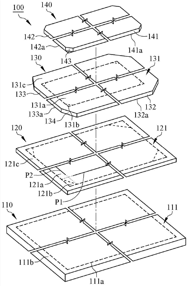
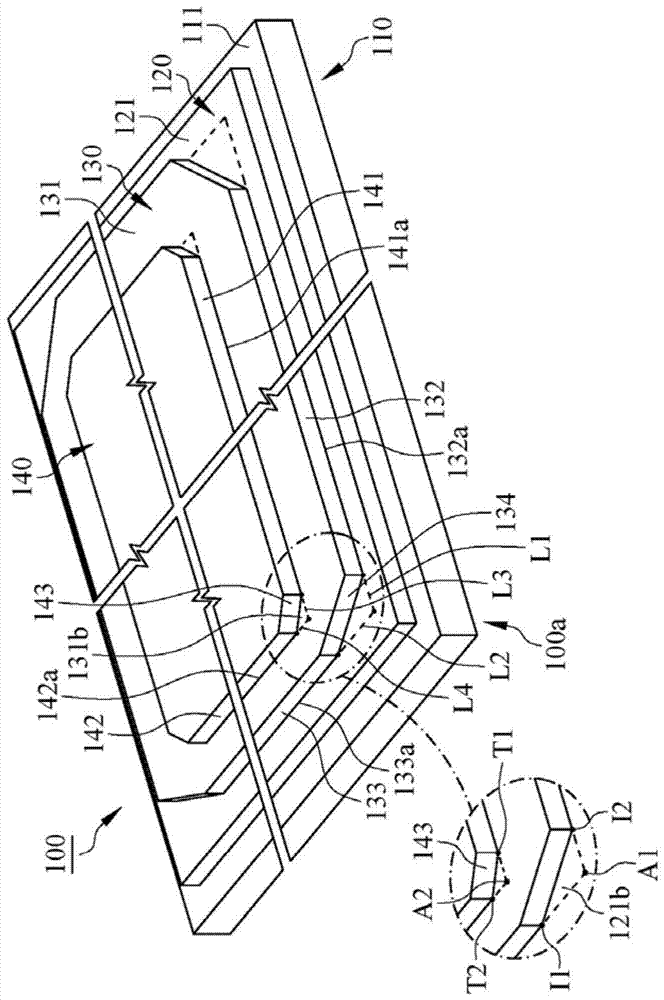
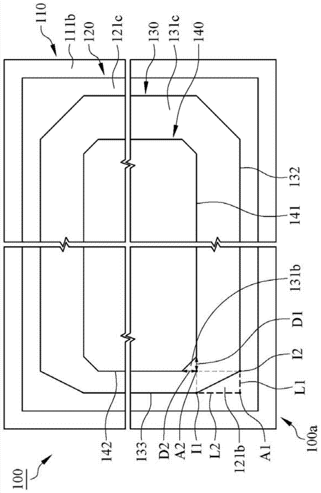
[0024] see figure 1 and figure 2 , which is a first preferred embodiment of the present invention, a semiconductor structure 100 has a corner 100a, the semiconductor structure 100 includes a carrier 110, a first protection layer 120, a second protection layer 130 and a third protection layer 140, The carrier 110 has a carrier surface 111, the carrier surface 111 has a protective layer setting area 111a and a protective layer exposed area 111b located outside the protective layer setting area 111a, the first protective layer 120 is set on the protective layer setting area 111a, the T...


PUM


Abstract

The present invention relates to a semiconductor structure, comprising a carrier, a first protection layer, a second protection layer and a third protection layer, the first surface of the first protection layer has a first anti-stress region, the second protection layer The first anti-stress region is exposed, the second protective layer has a first side and a second side, a first extension line extending from the first bottom of the first side and a second bottom of the second side The extended second extension lines intersect to form a first base point, the third protective layer has a third side and a fourth side, the third side forms a first projection line on the first surface, and the first projection line The extension line intersects with the second base to form a first intersection point, the fourth side surface forms a second projection line on the first surface, and the extension line of the second projection line intersects with the first base to form a second intersection point. The area formed by the intersection point, the first base point, the first intersection point and the second intersection point is the first anti-stress area.

Description

technical field [0001] The present invention relates to a semiconductor structure, in particular to a semiconductor structure with an anti-stress region. It is a new design with considerable practicability and progressiveness, and is suitable for wide popularization and application in the industry. Background technique [0002] see Figure 6 , is a conventionally known semiconductor structure 200, which has a carrier 210, a first protective layer 220, a second protective layer 230, and a third protective layer 240, because the first protective layer 220, the second protective layer 230 and the third protective layer 240 are quadrangular and the first protective layer 220, the second protective layer 230 and the third protective layer 240 are stacked on the carrier 210, so the stress of the semiconductor structure 200 is easy to concentrate on The overlapping corner of the first passivation layer 220 and the second passivation layer 230 makes the corner of the overlap of the...

Claims


Application Information

Patent Timeline
Patent Type & Authority Patents(China)
IPC IPC(8): H01L29/06
CPCH01L23/3192H01L23/562H01L2924/0002H01L2924/00H01L23/58H01L23/28H01L23/53295
Inventor 谢庆堂徐佑铭刘明升王智平
Owner CHIPBOND TECH
Why Eureka
Try Eureka