Infiltrating type micro-image exposal apparatus and method thereof

A kind of equipment and lithography technology, which is applied in the direction of microlithography exposure equipment, photolithography exposure device, electrical components, etc., can solve the problems of circuit pattern image distortion and achieve the effect of improving quality

Inactive Publication Date: 2007-05-16
TAIWAN SEMICON MFG CO LTD
View PDF0 Cites 28 Cited by
  • Summary
  • Abstract
  • Description
  • Claims
  • Application Information

AI Technical Summary

Problems solved by technology

These residual micro-bubbles tend to attach to the surface of the photoresist, which is typicall

Method used


Image

  • Infiltrating type micro-image exposal apparatus and method thereof
  • Infiltrating type micro-image exposal apparatus and method thereof
  • Infiltrating type micro-image exposal apparatus and method thereof

Examples


Embodiment Construction

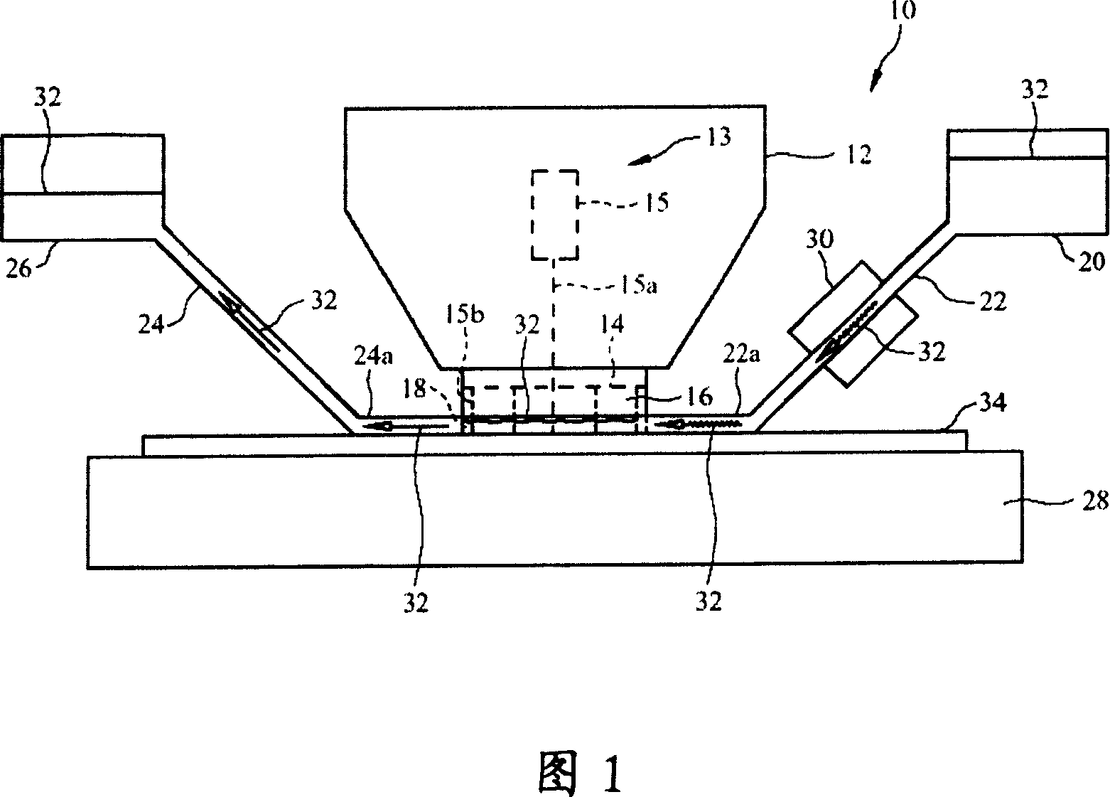
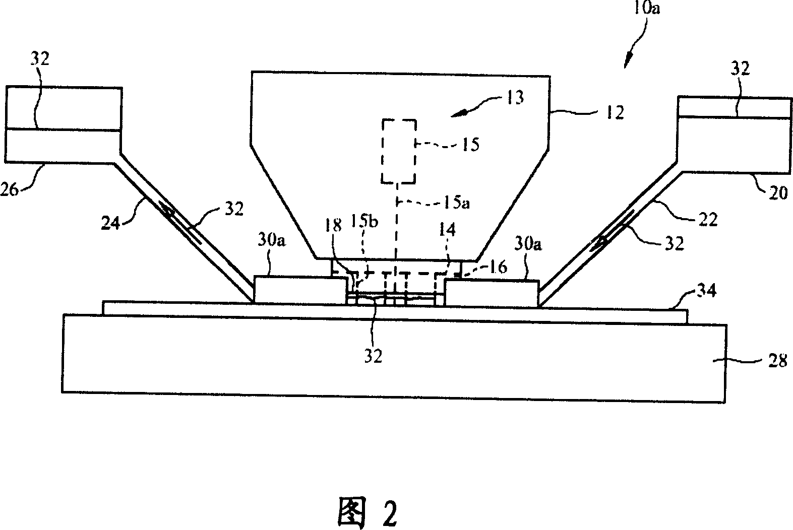
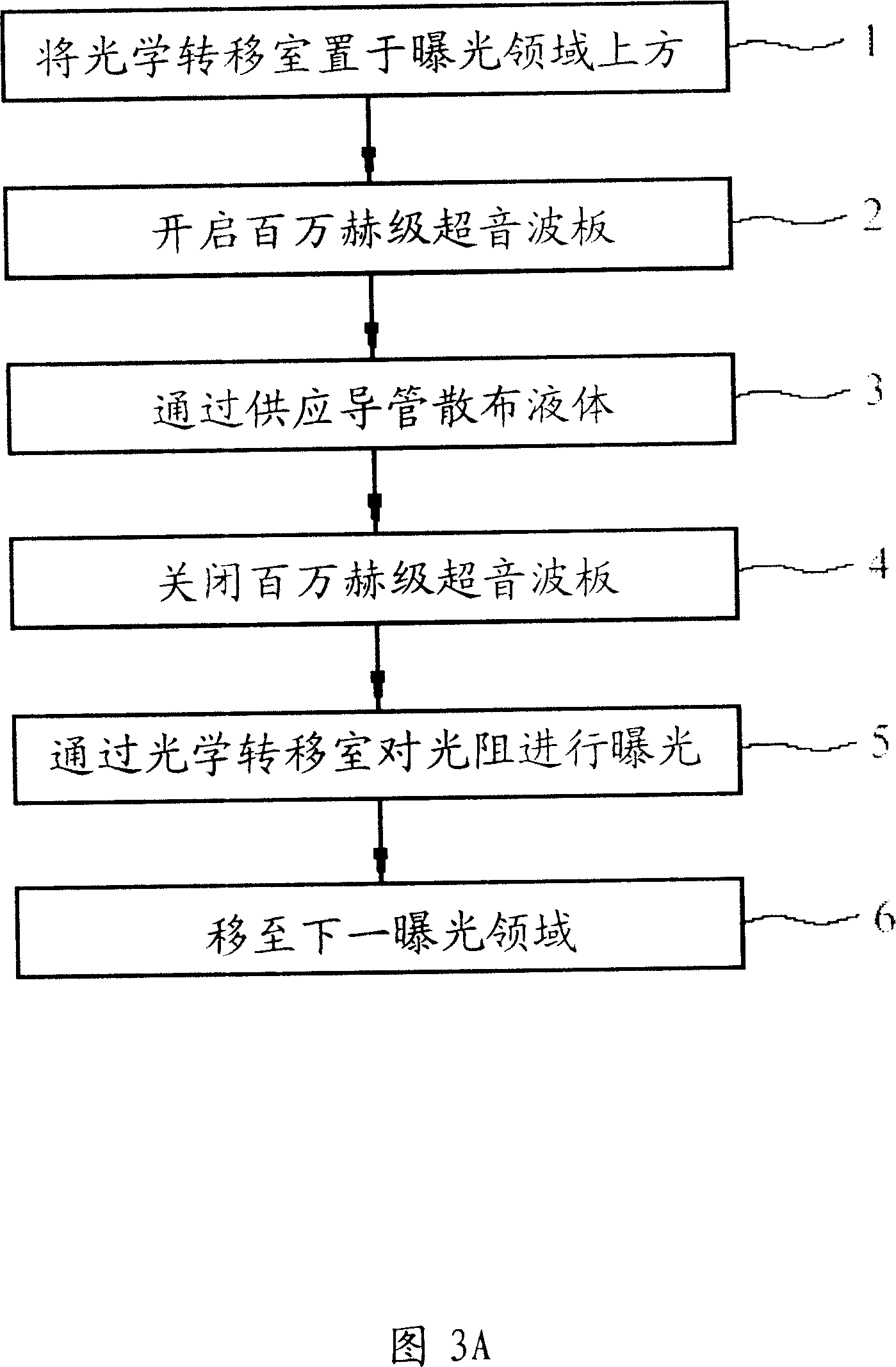
[0096] In order to further explain the technical means and effects of the present invention to achieve the intended purpose of the invention, the specific implementation, structure and method of the immersion lithography exposure equipment and method proposed according to the present invention will be described below in conjunction with the accompanying drawings and preferred embodiments. , steps, features and effects thereof are described in detail below.

[0097] The present invention is to develop a novel megasonic ultrasonic immersion lithography exposure equipment for substantially eliminating microbubbles from exposure liquid before, during, or both before and during immersion lithography. In one embodiment, the apparatus includes an optical box in which a mask and a lens are mounted. An optical transfer chamber is provided below the lens of the optical box. The inlet conduit communicates with the optical transfer chamber to distribute the immersion liquid into the opti...


PUM


Abstract

This invention relates to one dipped micro image exposure device and its method, which is suitable for dipped micro image bubble elimination during exposure period and comprises optical system to project light onto crystal circle through light cover and optical transfer chamber is near to above optical system to load exposure liquid; at least one million Hertz super wave board to combine to optical transfer chamber to generate sound wave to eliminate exposure micro bubble.

Description

technical field [0001] The invention relates to a lithography process, which is applied in the manufacture of semiconductor integrated circuits to make integrated circuit patterns on photoresists, and in particular to a megasonic ultrasonic immersion lithography exposure equipment and method, wherein the infiltration liquid Sonicated to eliminate air bubbles in the liquid during the lithographic exposure step. Background technique [0002] In general, various processing steps are used to fabricate integrated circuits on semiconductor wafers. These steps include: depositing a conductive layer on the silicon wafer buildup; forming a photoresist or other mask, such as titanium oxide or silicon oxide, with the desired metal interconnect pattern using standard lithography or optical lithography techniques; The round substrate undergoes a dry etching process to remove the conductive layer from areas not covered by the mask, thus etching the conductive layer on the substrate in th...

Claims


Application Information

Patent Timeline
IPC IPC(8): G03F7/20H01L21/027
Inventor 张庆裕林建宏林进祥鲁定中林本坚
Owner TAIWAN SEMICON MFG CO LTD
Why Eureka
Try Eureka