Light-emitting diode

A light-emitting diode and chip technology, which is applied in the direction of electrical components, electric solid-state devices, circuits, etc., can solve the problems of light energy loss, reduce the light output efficiency of light-emitting diodes, etc., and achieve the effect of improving light output efficiency and reducing total reflection phenomenon

Active Publication Date: 2015-03-18
ZHANJING TECH SHENZHEN +1
View PDF5 Cites 6 Cited by
  • Summary
  • Abstract
  • Description
  • Claims
  • Application Information

AI Technical Summary

Problems solved by technology

However, the refractive index of the existing packaging material is about 1.4-1.5. According to the law of refraction, for example, when the refractive index of the packaging material is 1.5 and the incident angle is greater than 41 degrees, the light will be totally reflected at the interface between the air and the packaging material, and then For example, when the refractive index of the p

Method used


Image

  • Light-emitting diode
  • Light-emitting diode
  • Light-emitting diode

Examples


Example Embodiment

[0015] The present invention will be further described in detail below in conjunction with the accompanying drawings.

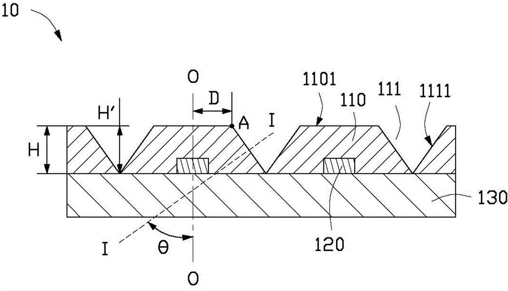
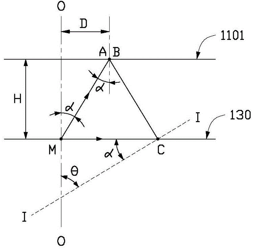
[0016] See figure 1 The light-emitting diode 10 provided by the present invention includes a substrate 130 having a circuit structure, at least one light-emitting diode chip 120 and a packaging material 110. The light emitting diode chip 120 is disposed on the substrate 130 and is electrically connected to the circuit structure of the substrate 130. The electrical connection mode of the circuit structure of the light-emitting diode chip 120 and the substrate 130 can be a wire bonding connection or a flip chip connection. The substrate 130 may be a PCB substrate, a ceramic substrate, a metal substrate, or a flexible substrate. The packaging material 110 covers the light emitting diode chip 120. The refractive index of the packaging material 110 is 1.4-1.5. The packaging material 110 may include a fluorescent substance.

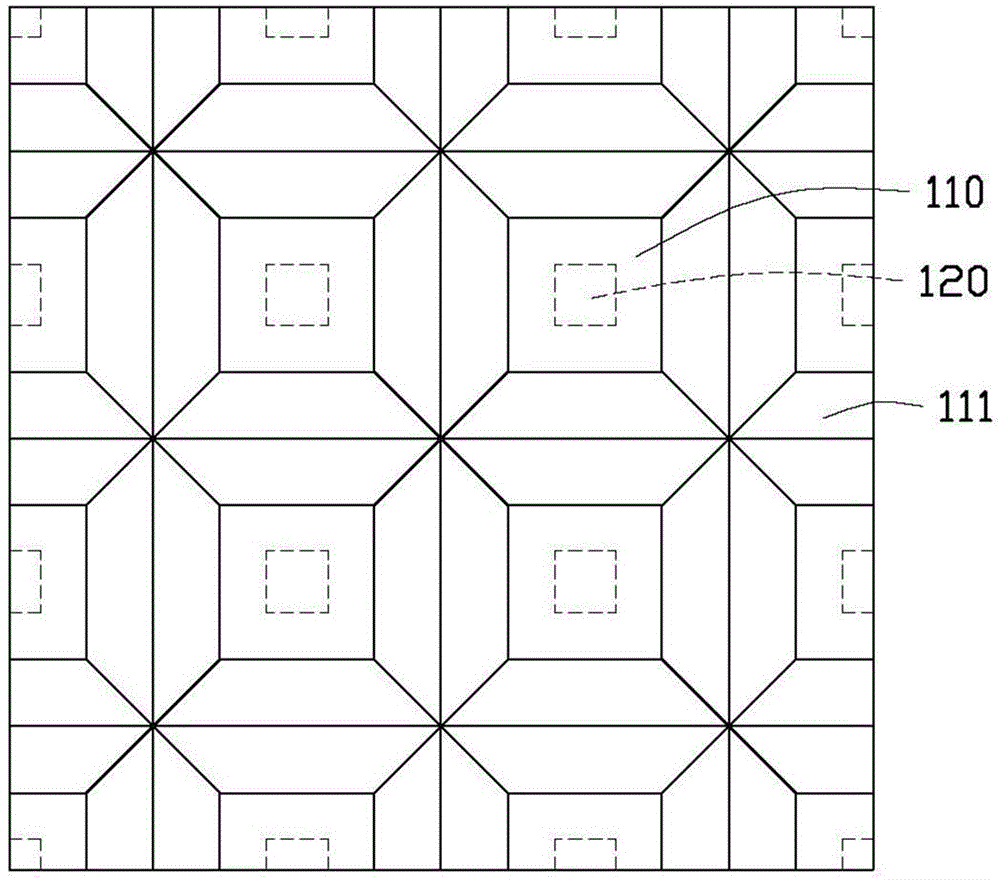
[0017] The packaging material 110 includ...


PUM


Abstract

An light emitting diode (LED) module includes a circuit board, a set of LED chips formed on and electrically connected to the circuit board, and an encapsulant arranged on the circuit board and covering the LED chips, a set of first recesses defined in a top surface of the encapsulant.

Description

Technical field [0001] The invention relates to a light-emitting diode, in particular to an integrated package light-emitting diode. Background technique [0002] As a new type of light source, light-emitting diodes have been widely used in many occasions. Over the years, the development direction of light-emitting diodes is still dedicated to the improvement of luminous efficiency. The influencing factors of luminous efficiency generally include the selected light-emitting diode chip material, the design of the component structure, transparency and total reflection. [0003] The most important component in the light emitting diode package is the light emitting diode chip, which determines the performance of the light emitting diode. In the prior art, the LED chip is usually coated with a packaging material to further protect the characteristics of the die. However, the refractive index of the existing packaging material is about 1.4-1.5. According to the law of refraction, for e...

Claims


Application Information

Patent Timeline
IPC IPC(8): H01L33/48H01L33/54
CPCH01L33/54H01L25/0753H01L2924/0002
Inventor 张忠民张简千琳吴雅婷杨政华
Owner ZHANJING TECH SHENZHEN
Why Eureka
Try Eureka