
Pattern optimized LED substrate with cone cluster type patterns and LED chip

A graphics-optimized substrate and cone cluster technology, applied in electrical components, circuits, semiconductor devices, etc., can solve the problems of limiting the promotion and application of LED chips on nano-scale graphics substrates, high manufacturing costs of nano-scale patterns, and reducing the life of LED chips, etc. problem, to achieve the effect of improving external quantum efficiency, reducing processing difficulty, and increasing reflection area

Active Publication Date: 2015-03-25
SOUTH CHINA UNIV OF TECH
View PDF6 Cites 0 Cited by
  • Summary
  • Abstract
  • Description
  • Claims
  • Application Information

AI Technical Summary

Problems solved by technology

Studies have shown that as the pattern pitch decreases, voids are likely to appear at the interface between GaN and sapphire due to the lack of time for GaN growth to heal, and cause more dislocations in the epitaxial layer. Even if the light extraction efficiency is improved, the epitaxial layer position The increase of errors will reduce the LED chip life
In addition, the high cost of manufacturing nanoscale patterns and difficulties in industrialization greatly limit the promotion and application of nanoscale patterned substrate LED chips

Method used


Image

  • Pattern optimized LED substrate with cone cluster type patterns and LED chip
  • Pattern optimized LED substrate with cone cluster type patterns and LED chip
  • Pattern optimized LED substrate with cone cluster type patterns and LED chip

Examples


Embodiment 1

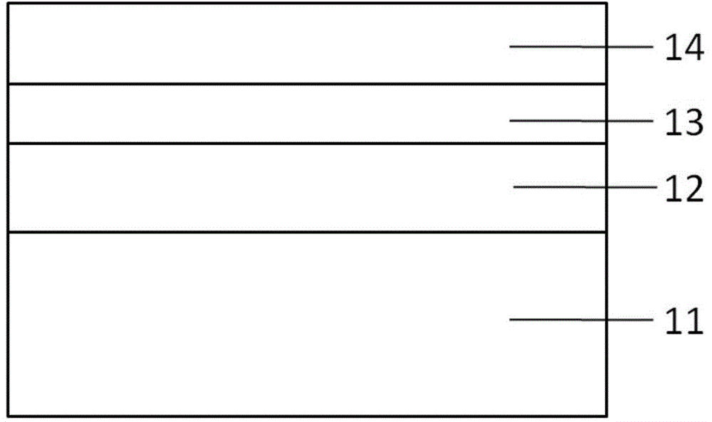
[0031] figure 1 It is a schematic diagram of the LED chip of this embodiment, which is composed of LED pattern optimized substrate 11, N-type GaN layer 12, MQWs quantum well layer 13, and P-type GaN layer 14 arranged in sequence.

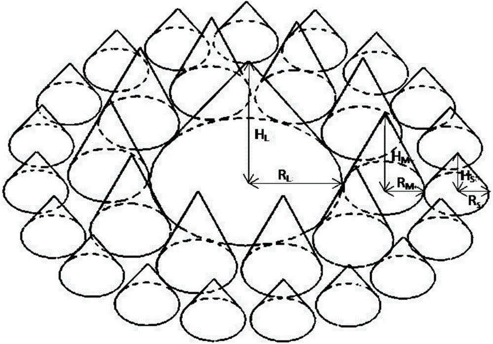
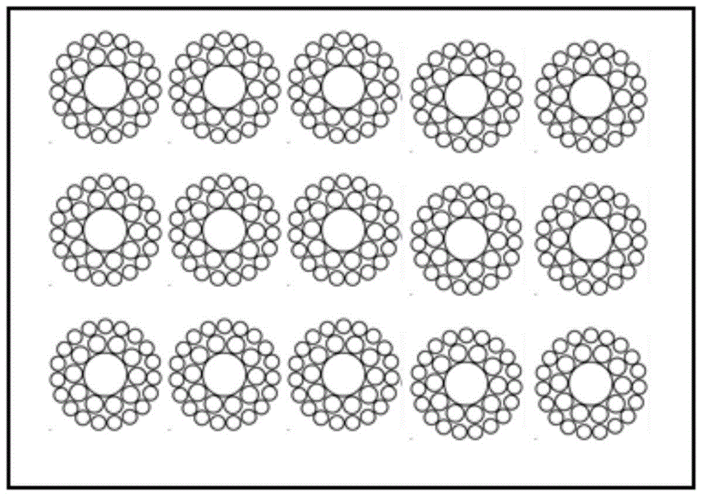
[0032] Such as figure 2 As shown, the pattern of the substrate in this embodiment consists of a plurality of conical clusters of the same shape arranged on the surface of the substrate in a rectangular arrangement. Such as image 3 As shown, each cone cluster is composed of a large cone, multiple medium cones and multiple small cones; the multiple medium cones are arranged in a circle around the large cone to form a medium cone circle; the multiple small cones surround the medium cone The circles are arranged in a circle to form small cone circles; the height H of each large cone L 2.0μm, bottom surface radius R L is 1.2μm; the height H of each middle cone M 1.25μm, bottom radius R M is 0.5μm; the height H of each small cone S 0.67μm, bottom...

Embodiment 2

[0034] The LED chip of this embodiment is composed of a conical cluster pattern LED pattern optimized substrate, an N-type GaN layer, an MQWs quantum well layer, and a P-type GaN layer arranged in sequence.

[0035] Such as Figure 4 As shown, the pattern of the substrate in this embodiment consists of a plurality of conical clusters of the same shape arranged on the surface of the substrate in a hexagonal arrangement. Each cone cluster is made up of a large cone, multiple medium cones and multiple small cones; the multiple medium cones are arranged in a circle around the large cone to form a medium cone circle; the multiple small cones are arranged in a circle around the medium cone circle circle, forming a small cone circle; the height H of each large cone L 1.0μm, bottom radius R L is 0.6μm; the height H of each middle cone M 0.75μm, bottom radius R M 0.25μm; the height H of each small cone S 0.3μm, bottom radius R S is 0.15 μm; the edge distance d of adjacent cone cl...

Embodiment 3

[0037] This embodiment is the same as Embodiment 1 except for the following features.

[0038] A plurality of cone clusters with the same shape in this embodiment adopt such as Figure 5 The rhombus arrangement shown.


PUM


Abstract

The invention discloses a pattern optimized LED substrate with cone cluster type patterns. The pattern of the substrate is formed by multiple cone clusters identical in shape, and the cone clusters are distributed on the surface of the substrate. Each cone clusters comprise a large cone, multiple middle cones and multiple small cones, wherein the multiple middle cones surround the large cone by a circle to form a middle cone ring, and the multiple small cones surround the middle cones surround the small cones by a circle to form a small cone ring. Compared with the prior art, the pattern optimized LED substrate has a higher light emitting efficiency than a common substrate LED chip, the cone clusters increase the reflection area and have a remarkable gain effect on light emitting at the bottom, and the pattern optimized LED substrate is particularly suitable for flip chip packaging. Target patterns can be easily obtained in actual processing, and the pattern optimized LED substrate is convening to apply and popularize.

Description

technical field [0001] The invention relates to an LED graphic optimized substrate, in particular to an LED graphic optimized substrate with a conical cluster pattern and an LED chip. Background technique [0002] GaN-based LEDs have the advantages of high brightness, low energy consumption, and long life, and are widely used in fields such as full-color displays and general lighting. However, the current GaN-based LED preparation technology cannot realize its full potential. The efficacy of general commercial LEDs is about 130lm / W, which is far lower than the theoretical maximum efficacy of LEDs of 360lm / W. The factors that limit the improvement of LED efficacy mainly involve two aspects, namely, the internal quantum efficiency and light extraction rate of LEDs. On the one hand, there is a lattice mismatch of about 16% and a thermal expansion coefficient mismatch of about 26% between the GaN epitaxial layer and the sapphire epitaxial substrate, making the GaN epitaxial lay...

Claims


Application Information

Patent Timeline
Patent Type & Authority Applications(China)
IPC IPC(8): H01L33/22H01L33/10
CPCH01L33/10H01L33/22
Inventor 李国强钟立义林志霆乔田周仕忠王海燕王凯诚
Owner SOUTH CHINA UNIV OF TECH
Learn More