Processing method for thin encapsulation substrate positioning hole

A processing method and technology for positioning holes, which are applied in metal processing and other directions, can solve problems such as easy damage, affect production yield, and unacceptable quality, increase overall thickness, improve damage problems, and avoid solder mask cracks or substrates. glitch effect

Inactive Publication Date: 2015-04-08
GUANGZHOU FASTPRINT CIRCUIT TECH +2
View PDF11 Cites 0 Cited by
  • Summary
  • Abstract
  • Description
  • Claims
  • Application Information

AI Technical Summary

Problems solved by technology

[0003] At present, when producing products with a plate thickness below 0.15mm, the scrapping rate of positioning holes is very high, and the scrapping rate of individual models exceeds 50%, which seriously affects the production yield;
[0004] For PCB, there are two ways to process positioning holes on double-sided panels. One is to process positioning holes in the outer layer drilling process, and then go through electroplating, external light imaging, solder mask, gold plating and other processes, and finally reach the shape process. The ring of the positioning hole is made of base material resin, and the overall thickness of the positioning hole is much smaller than the thickness of the finished product, so it is easy to be damaged during the upper and lower boards in the shape process; another way is to increase the second drilling process when the product reaches the shape process , use a drilling machine to process the positioning hole. This method can increase the overall thickness of the positioning hole because the positioning hole does not need to be opened. The burr problem of the material is unacceptable for packaging substrate products;

Method used


Image

  • Processing method for thin encapsulation substrate positioning hole
  • Processing method for thin encapsulation substrate positioning hole
  • Processing method for thin encapsulation substrate positioning hole

Examples


Embodiment Construction

[0032] The present application will be further elaborated below through specific examples.

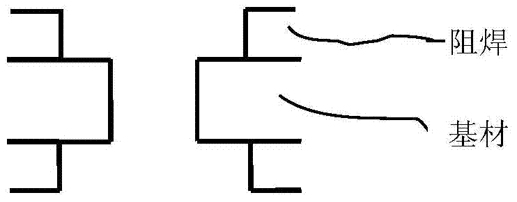
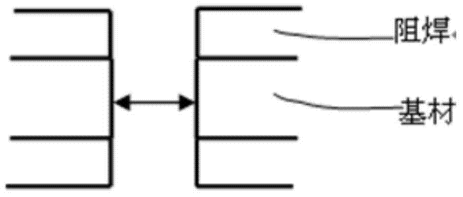
[0033] In this embodiment, a processing method for positioning holes of a packaging base sheet, the preparation method of the packaging base sheet includes the following steps: drilling, electroplating, outer layer photoimaging, solder masking, gold plating, and contouring processes; the packaging base sheet Thickness≤0.2mm.

[0034] The processing method of positioning hole comprises the following steps (as image 3 shown):

[0035] Making positioning hole targets: in the outer photoimaging or solder mask process, making targets at the positions of the positioning holes on the board surface; the number of the targets matches the number of positioning holes;

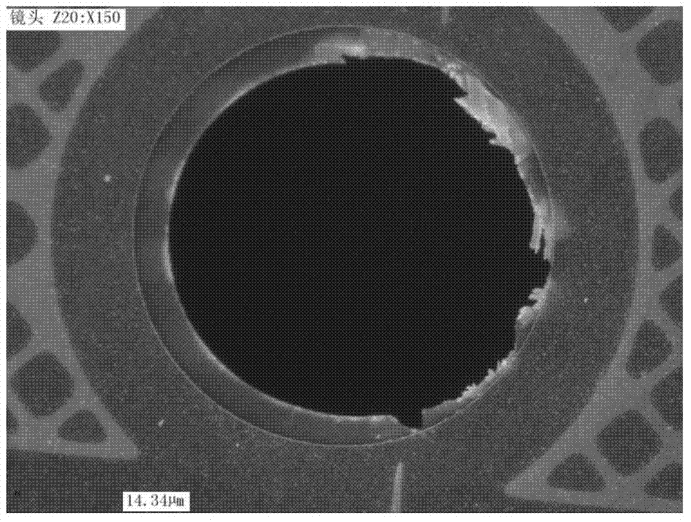
[0036] Positioning hole processing: In the shape process, a punching machine is used to process positioning holes.

[0037] The steps of the punching machine processing positioning holes are:

[0038] The CCD (optical lens) o...


PUM

PropertyMeasurementUnit
Thicknessaaaaaaaaaa

Abstract

The invention discloses a processing method for a thin encapsulation substrate positioning hole. A preparation method for a thin encapsulation substrate comprises the following steps: drilling, electroplating, outer-layer light imaging, resistant welding, gold plating and appearance forming. The processing method for the positioning hole comprises the following steps: manufacturing a positioning hole target: manufacturing a target at a positioning hole position on the plate surface in the outer-layer light imaging or resistant welding working procedure; positioning hole processing: processing the positioning hole by a punching machine in the appearance forming working procedure. According to the positioning hole processing method disclosed by the invention, the whole thickness of the positioning hole is greatly increased, and the problem of breakage of an upper appearance plate and a lower appearance plate of the thin plate positioning hole during milling is effectively solved; special punching equipment is used in the positioning hole processing method, so that the problem of resisting welding breakage or base material burrs caused by processing by a drilling machine can be effectively solved.

Description

technical field [0001] The invention relates to the technical field of printed circuit boards, in particular to a processing method for a positioning hole of a packaging substrate sheet. Background technique [0002] The thickness range of packaging substrate products is generally 0.1-0.8mm, which is much smaller than that of PCB products; especially for double-sided panels with a product thickness below 0.2mm, since the overall thickness of the positioning holes is only 30-70um (such as figure 1 As shown), a slight collision during the milling process of the upper and lower plates will cause damage to the positioning hole, resulting in a large number of scrapped units (the photo of the damaged positioning hole of the scrapped plate is shown in figure 2 shown); [0003] At present, when producing products with a plate thickness below 0.15mm, the scrapping rate of positioning holes is very high, and the scrapping rate of individual models exceeds 50%, which seriously affect...

Claims


Application Information

Patent Timeline
IPC IPC(8): B26F1/02
CPCB26F1/02
Inventor 卢汝峰梁汉洙谢添华
Owner GUANGZHOU FASTPRINT CIRCUIT TECH
Why Eureka
Try Eureka