Supercharge Your Innovation With Domain-Expert AI Agents!

Flash chip combined with fpga and instruction processing method

A chip and external instruction technology, applied in machine execution devices, digital data authentication, etc., can solve the problems of high design complexity, high design cost, low work efficiency, etc., and achieve the effect of strong versatility, low cost, and improved performance

Active Publication Date: 2018-08-03
GIGADEVICE SEMICON (BEIJING) INC
View PDF9 Cites 0 Cited by
  • Summary
  • Abstract
  • Description
  • Claims
  • Application Information

AI Technical Summary

Problems solved by technology

[0006] The technical problem to be solved by the present invention is to provide a FLASH chip combined with an FPGA and an instruction processing method to solve the problems of high design complexity, long design cycle, high design cost, weak versatility, and low work efficiency.

Method used


Image

  • Flash chip combined with fpga and instruction processing method
  • Flash chip combined with fpga and instruction processing method

Examples


Embodiment Construction

[0040] In order to make the above objects, features and advantages of the present invention more comprehensible, the present invention will be further described in detail below in conjunction with the accompanying drawings and specific embodiments.

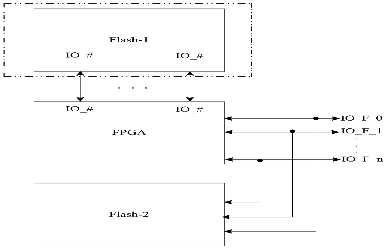
[0041] One of the core ideas of the embodiments of the present invention is that the FLASH chip combined with the FPGA includes a Field Programmable Gate Array FPGA, the first memory chip Flash-1, and the second memory chip Flash-2; Flash-1 and FPGA each include Internal IO pins, the internal IO pins of the Flash-1 are interconnected with the internal IO pins of the FPGA, and the FPGA and the Flash-1 are internally interconnected through interconnected internal IO pin pairs Communication; the FPGA is connected to the same IO pin in the Flash-2, and is connected to the same external shared pin of the chip; external instructions are transmitted to the Flash-2 and the in the FPGA. In the embodiment of the present invention, the exis...


PUM


Abstract

The present invention provides a kind of FLASH chip combined with FPGA, said FPGA and Flash-1 carry out internal mutual communication through interconnected internal IO pin pair; Described FPGA is connected with the same IO pin in Flash-2 , and be connected to the same external shared pin of the chip; the external command is transmitted to the Flash-2 and the FPGA through the external shared pin of the chip, and the Flash-2 and the FPGA respectively judge whether to execute the external command; if Described external instruction is the RPMC verification instruction that described Flash-2 cannot recognize, then FPGA generates the first RPMC verification value according to configuration information and the value of RPMC, and judges whether it is consistent with the second RPMC verification value in the RPMC verification instruction; if If they are inconsistent, the chip is an illegal chip. The invention is used to solve the problems of high design complexity, long design cycle, high design cost, weak versatility, and low work efficiency.

Description

technical field [0001] The invention relates to the field of chip technology, in particular to a FLASH chip combined with an FPGA and an instruction processing method. Background technique [0002] RPMC (Replay Protection Monotonic Counter) is a new function of the Basic Input-Output System (BIOS) chip promoted by Intel. It contains a high-capacity Flash chip and RPMC circuit. Among them, the capacity of the Flash chip is 8M, 16M, 32M, 64M, 128M, 256M or higher, and is used to store the code and data of the CPU BIOS; the RPMC circuit ensures the confidentiality and integrity of the read and write data. The RPMC circuit and its integrated FLASH constitute the hardware platform of the BIOS in the personal computer (Personal Computer, PC) system. [0003] When designing a FLASH chip with RPMC function, designers usually integrate large-capacity Flash and RPMC on one chip, that is, RPMC circuit and Flash are designed together. [0004] However, this design method has the foll...

Claims


Application Information

Patent Timeline
Patent Type & Authority Patents(China)
IPC IPC(8): G06F9/30G06F21/44
Inventor 张新楼潘荣华张赛
Owner GIGADEVICE SEMICON (BEIJING) INC
Features
  • R&D
  • Intellectual Property
  • Life Sciences
  • Materials
  • Tech Scout
  • Unparalleled Data Quality
  • Higher Quality Content
  • 60% Fewer Hallucinations
Learn More