A peec-based simulation method for electromagnetic screen effect of chassis with connecting accessories
A simulation method and electromagnetic simulation technology, applied in electrical digital data processing, special data processing applications, instruments, etc., can solve problems such as inability to correctly reflect contributions, achieve accurate electromagnetic compatibility analysis models of chassis, shorten calculation time, and simplify numerical values effect of the model
- Summary
- Abstract
- Description
- Claims
- Application Information
AI Technical Summary
Problems solved by technology
Method used
Image
Examples
Embodiment 1
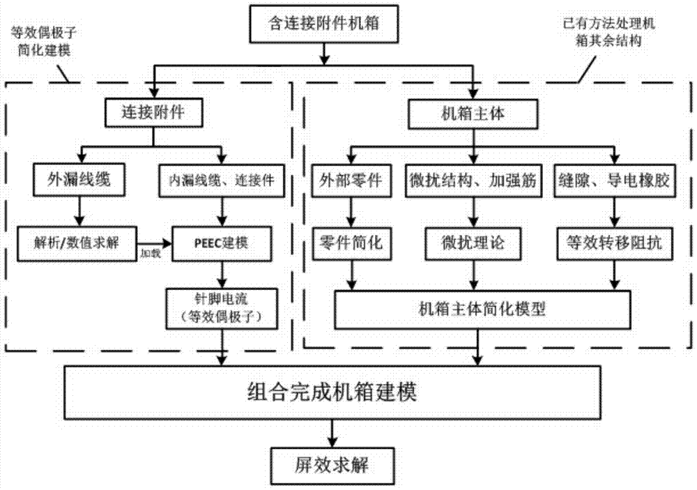
[0042] a kind of like figure 1 As shown, the PEEC-based simulation method for the electromagnetic screen effect of the chassis with connection accessories includes the following steps:
[0043] Step 101, divide the chassis containing the connection accessories into two sub-domains: the chassis main body and the connection accessories;
[0044] Step 102, for different sub-domains and objects, based on their characteristics in the electromagnetic compatibility analysis, using different modeling simplification methods to establish electromagnetic simulation numerical models of each part;
[0045] Step 103, after establishing the electromagnetic compatibility analysis numerical models of the connecting accessories and the chassis main body through step 102, combine the complete chassis electromagnetic simulation model, the combination principle is:
[0046]
[0047] To meet the conditions:
[0048]
[0049] in is the nth pin i line element of the m connector, P mni Its ...
Embodiment 2
[0067] 1. Simulation object
[0068] select as Figure 4 The shown case model is used for electromagnetic screen effect simulation, in which the shape and structure parameters are L×W×H=400mm×312mm×325mm, and the cable diameter is 1mm, which is located inside the shielded box Ω 1 The length of the cable is l 1 =10mm, outside the shielded box Ω 2 The length of the cable is l 2 =490mm. The GJB599 series 7-pin plug JY2476T11F99P-H, which is common in national defense and aerospace electronic products, is located in the center of the front panel, and the diameter of the conductive copper core is 1.1mm. The 10mm×10mm×10mm metal perturbation structure is located at the corner as shown in the figure, the rib width c=10mm, the thickness is 5mm, and the ventilation hole array is located as Figure 4 The position shown is 25mm away from both sides, and is composed of a 6*6 circular hole array with a diameter of 4mm and an interval of 2mm. The observation point P(100,150,85) is loc...
PUM
 Abstract
Description
Claims
Application Information


