Fingerprint recognition sensor

A technology of fingerprint identification and sensor devices, which is applied in the field of microelectronics packaging, can solve problems such as complex process steps, adverse effects on final product yield and reliability, and increased manufacturing costs

Inactive Publication Date: 2015-05-06
HUATIAN TECH XIAN
View PDF7 Cites 16 Cited by
  • Summary
  • Abstract
  • Description
  • Claims
  • Application Information

AI Technical Summary

Problems solved by technology

As the number of discrete components increases, the process steps become more and more complex, and the manufacturing cost increases. At the same time, it has an adverse effect on the yield and reliability of the final product, and the assembly or packaging process of discrete components is time-consuming and inefficient.

Method used


Image

  • Fingerprint recognition sensor
  • Fingerprint recognition sensor

Examples


no. 1 example

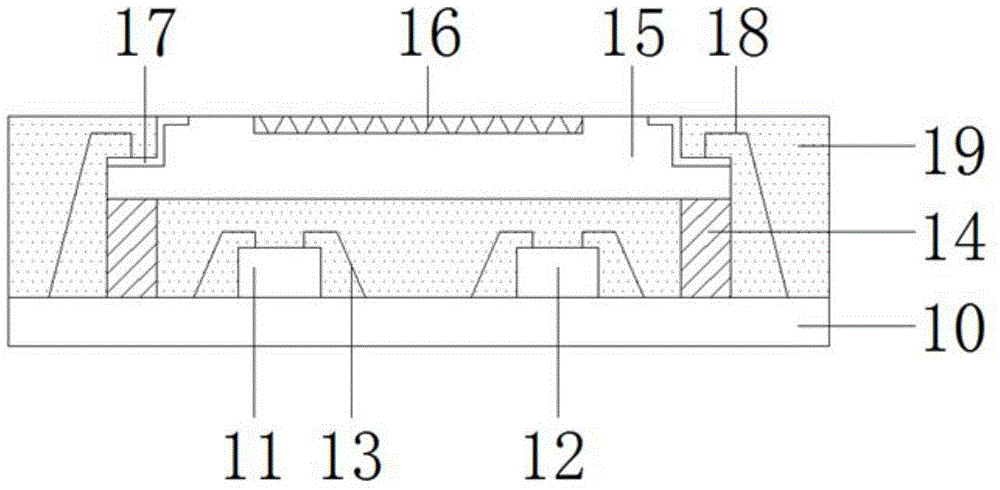
[0016] figure 1 It is a schematic cross-sectional view of the fingerprint recognition sensor device according to the first embodiment of the present invention.

[0017] Please refer to figure 1 The fingerprint identification sensor device includes a substrate 10, which may be a printed circuit board, a ceramic body or similar structures, and the substrate 10 has a solder ball interconnection structure (not shown in the figure) formed on its lower surface. At least one chip is disposed on the upper surface of the substrate 10 through an adhesive material (not shown in the figure). In this embodiment, at least one chip can be a memory chip 11 and an ASIC chip 12, and the bonding material can be a commonly used polymer bonding material, silica gel, epoxy resin, benzocyclobutene, solder, etc. . The memory chip 11 and the ASIC chip 12 are bonded to the upper surface of the substrate 10 through the first metal wire 13 .

[0018] At least one embankment 14 is configured on the up...

no. 2 example

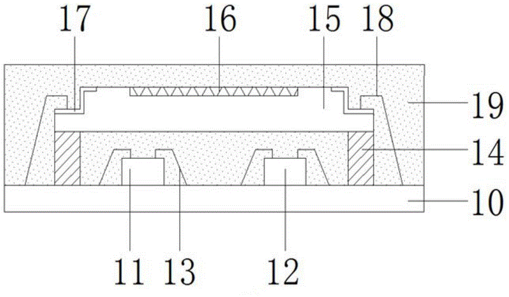
[0022] figure 2 It is a schematic cross-sectional view of the fingerprint recognition sensor device according to the second embodiment of the present invention.

[0023] Please refer to figure 2 , the second embodiment with figure 1 The difference of the first embodiment shown is that the upper surface of the fingerprint identification sensor chip 15 having the sensor element array 16 is covered by the plastic encapsulation material 19, and the thickness of the plastic encapsulation material 19 on the upper surface of the fingerprint identification sensor chip 15 is 20 Micron to 120 microns, the Mohs hardness of the molding material 19 is greater than or equal to 5H, so as to ensure that it has sufficient hardness to effectively protect the fingerprint identification sensor chip 15 and the sensor element array 16 located thereon. Meanwhile, in order to improve the sensing accuracy and sensitivity of the sensor element array 16 , the dielectric constant of the molding mater...


PUM


Abstract

The invention discloses a fingerprint recognition sensor, and belongs to the technical fields of integrated circuit encapsulating and sensor. The fingerprint recognition sensor comprises a substrate, at least one chip arranged on the upper surface of the substrate, at least one embankment wall which is arranged on the upper surface of the substrate to limit the position of the at least one chip, and a fingerprint recognition sensor chip which is arranged on the surface of the embankment wall; a groove in which a conductor layer is arranged is formed in the side edge of the upper surface of the fingerprint recognition sensor; a plastic encapsulating material exposes from the upper surface of the fingerprint recognition sensor chip or the upper surface of the fingerprint recognition sensor chip is thinly wrapped with the plastic encapsulating material. With the adoption of the fingerprint recognition sensor, the encapsulating size can be reduced, and moreover, the encapsulating process is simple, and the cost is low.

Description

technical field [0001] The invention relates to technologies such as microelectronic package technology, sensor technology and chip interconnection. Background technique [0002] With the continuous improvement of the intelligence of terminal products, various sensor chips emerge in endlessly. Sensor chips have expanded the application fields of smart phones, tablet computers and other products. For example, the emergence of fingerprint recognition chips has greatly improved the security of the above products. [0003] At present, a typical fingerprint identification sensor chip includes a semiconductor chip on which an array of sensor elements for sensing is formed as a sensing area. Its biggest feature is that the sensing area on the chip surface interacts with the user's finger to generate electric signal. In order to ensure the accuracy and sensitivity of sensing, the distance between the sensing area and the user’s finger should be as small as possible. According to t...

Claims


Application Information

Patent Timeline
Patent Type & Authority Applications(China)
IPC IPC(8): H01L23/498H01L23/31
CPCH01L2224/48227H01L2924/181H01L2924/00012
Inventor 夏国峰于大全
Owner HUATIAN TECH XIAN
Why Eureka
Try Eureka