

A reinforced isolation circuit
An isolation and circuit technology, applied in the field of wireless communication, to suppress loop distortion, improve isolation, and shorten turn-off delay time
- Summary
- Abstract
- Description
- Claims
- Application Information
AI Technical Summary
Problems solved by technology
Method used
Image

Examples
Embodiment 1
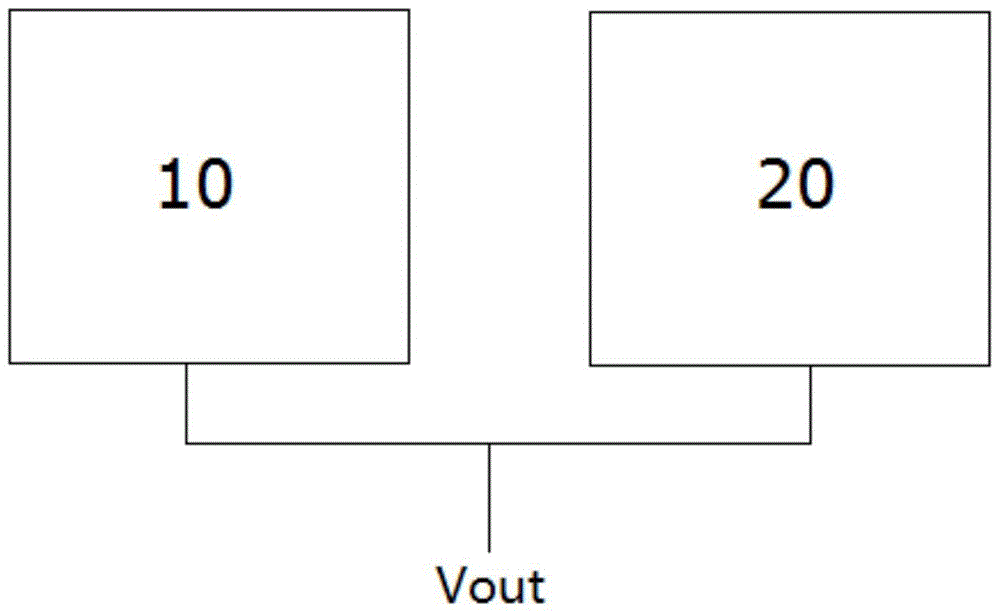
[0036] Such as image 3 As shown, the power supply circuit 10 of the enhanced isolation circuit is a p-MOS, its source is connected to the power supply VDD, the discharge circuit 20 is an n-MOS, its source is grounded, and the drain of the p-MOS is the voltage output of the discharge circuit 10 Terminal V out , which is connected to the drain of the n-MOS.
[0037] The inverter circuit 30 is an inverter 31 , and the Tx / Rx control signal Tx / Rx Enable Signal is respectively connected to the gates of the p-MOS and n-MOS through the inverter 31 .
[0038]The inverter 31 inverts the Tx / Rx control signal Tx / Rx Enable Signal, that is, inverts the high potential into a low potential to control whether the p-MOS and n-MOS are enabled or not. When the Tx / Rx control signal Tx / Rx Enable Signal is at a high potential, the potential is reversed to a low potential through the inverter 31. At this time, the p-MOS channel is turned on, and the output voltage terminal V of the power supply ci...
Embodiment 2
[0043] Such as Figure 4 As shown, the power supply circuit 10 of the enhanced isolation circuit is a pnp-BJT, its emitter is connected to the power supply VDD, the discharge circuit 20 is an npn-BJT, its emitter is grounded, and the collector of the pnp-BJT is the voltage of the discharge circuit 10 Output V out , which is connected to the collector of the npn-BJT.
[0044] The inverter circuit 30 is an inverter 31 , and the Tx / Rx control signal Tx / Rx Enable Signal is respectively connected to the bases of the pnp-BJT and the npn-BJT through the inverter 31 .
[0045] In Embodiment 2, the p-MOS and n-MOS in Embodiment 1 are replaced by pnp-BJT and npn-BJT respectively, which can also achieve the effect of shortening the discharge time. Since the start-up of p-MOS and n-MOS must first charge the gate oxide layer to reverse the polarity of the channel, there will be a voltage delay time t D , no voltage delay time t if npn-BJT is used D , ie t D =0. Of course, in order to...
Embodiment 3
[0047] Such as Figure 5 As shown, the power supply circuit 10 of the enhanced isolation circuit is a low dropout regulator (Low Drop-Outregulator, LDO), the discharge circuit 20 is an n-MOS, its source is grounded, and its drain is connected to the voltage output of the power supply circuit 10 Terminal V out connected. The Tx / Rx control signal Tx / Rx Enable Signal is connected to the low dropout voltage regulator LDO to control whether the low dropout voltage regulator LDO supplies power. At the same time, the Tx / Rx control signal Tx / Rx Enable Signal passes through an inverter 31 and n - the gates of the MOS are connected to control whether the discharge circuit 20 discharges.
[0048] When the Tx / Rx control signal Tx / Rx Enable Signal is at a high voltage level, the low dropout voltage regulator LDO can supply power; when the Tx / Rx control signal Tx / Rx Enable Signal is at a low voltage level, the low dropout voltage regulator The device LDO is powered off, and at this time ...
PUM
 Abstract
Description
Claims
Application Information