Pixel circuit and driving method thereof and display device

A technology for pixel circuits and driving transistors, applied in static indicators, instruments, etc., can solve problems such as long settling time, application of current-limited pixel circuits, and complex circuit structure driving signals.

Active Publication Date: 2015-05-20
PEKING UNIV SHENZHEN GRADUATE SCHOOL
View PDF9 Cites 17 Cited by
  • Summary
  • Abstract
  • Description
  • Claims
  • Application Information

AI Technical Summary

Problems solved by technology

The compensation accuracy of the current-type pixel circuit is relatively high, but it needs a relatively long settling time, especially in the case of low current and large parasitic capacitance on the data line
This severely limits the application of current-mode pixel circuits in large-area, high-resolution displays
The compensation accuracy of the voltage-type pixel circuit is not as high as that of the current-type pixel circuit, and the circuit structure or / and driving signal are generally relatively complicated, but the driving speed is fast
How to better sense the unevenness or drift of the threshold voltage of the driving transistor T1 and compensate for it, so as to reduce the display unevenness caused by the threshold voltage has become an urgent problem to be solved

Method used


Image

  • Pixel circuit and driving method thereof and display device
  • Pixel circuit and driving method thereof and display device
  • Pixel circuit and driving method thereof and display device

Examples


Embodiment 1

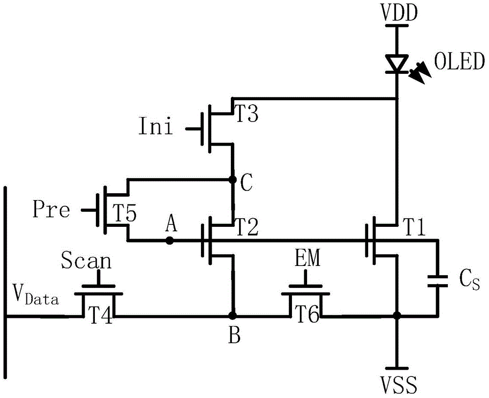
[0029] Please refer to figure 2 , which is a structure diagram of a pixel circuit disclosed in this embodiment, the pixel circuit is used to arrange scan lines arranged in the first direction for supplying scan signals and data lines arranged in the second direction for supplying data signals Between, in this embodiment, the first level terminal is the low level terminal V SS or ground wire, the second level terminal is the high level terminal V DD , the pixel circuit includes: a driving transistor T1, a light emitting element OLED, a storage capacitor Cs, a second transistor T2, a third transistor T3, a fourth transistor T4, a fifth transistor T5 and a sixth transistor T6, wherein,

[0030]The control electrode of the drive transistor T1 is coupled to the control electrode of the second transistor T2, such as figure 2 As shown, the coupling node is the first node A; the second pole of the driving transistor T1 is coupled to the second terminal of the light-emitting elemen...

Embodiment 2

[0051] Different from the above-mentioned embodiments, in the pixel circuit disclosed in this embodiment, each transistor is a P-channel thin film transistor, and the active level of each transistor is low. Please refer to Figure 4 , is a structure diagram of a pixel circuit disclosed in this embodiment.

[0052] The control electrode of the driving transistor T1 is coupled to the control electrode of the second transistor T2, and the coupling node is the first node A; the second electrode of the driving transistor T1 is coupled to the second end of the light emitting element OLED; the first end of the light emitting element OLED is used for coupled to the low-level terminal V SS , the first pole of the driving transistor T1 is used to couple to the high level terminal V DD . In this embodiment, the first end of the light emitting element OLED is a cathode, and the second end is an anode.

[0053] The first end of the storage capacitor Cs is coupled to the control electro...

Embodiment 3

[0068] Please refer to Image 6 , is a structural diagram of a pixel circuit disclosed in this embodiment. The difference from Embodiment 2 is that in the pixel circuit of this embodiment, the driving transistor T1 and the second transistor T2 are P-channel thin film transistors, and the third transistor T3, The fourth transistor T4, the fifth transistor T5 and the sixth transistor T6 are all N-channel thin film transistors. The active levels of the conduction of the driving transistor T1 and the second transistor T2 are low level; the active levels of the conduction of the third transistor T3 , the fourth transistor T4 , the fifth transistor T5 and the sixth transistor T6 are high level.

[0069] The control electrode of the driving transistor T1 is coupled to the control electrode of the second transistor T2, and the coupling node is the first node A; the second electrode of the driving transistor T1 is coupled to the second end of the light emitting element OLED; the first ...


PUM


Abstract

The invention provides a pixel circuit and a driving method thereof. The driving method comprises the following steps of in the initializing phase, conducting a third transistor, and initializing each electrode level of a second transistor; in the programming phase, storing threshold voltage and data signals of the second transistor into a storage capacitor, wherein the threshold voltage is used for representing the threshold voltage for driving the transistor; in the light emitting phase, enabling a driving transistor to generate driving current according to the differential voltage driving of the two ends of the storage capacitor, and drive a light emitting element to emit light. The driving method has the advantages that as the second transistor and the driving transistor are adjacently arranged in the pixel circuit and have the same grid voltages, the source voltages are uniform in the light emitting phase; the second transistor is capable of imaging the threshold voltage of the driving transistor in the initializing phase and the drift condition of the threshold voltage after use, and the threshold voltage is stored in the storage capacitor in the programming phase, so as to solve the problem of compensating the nonuniform threshold voltage or the threshold voltage drifting of the driving transistor in the light emitting phase. The invention also discloses a display device.

Description

technical field [0001] The present application relates to the field of display devices, in particular to a pixel circuit, a driving method thereof, and a display device. Background technique [0002] Due to the advantages of high brightness, high luminous efficiency, wide viewing angle and low power consumption, Organic Light-Emitting Diode (OLED) display has been extensively studied in recent years and has been rapidly applied to a new generation of displays. The OLED display can be driven in two ways: passive matrix OLED (PMOLED) and active matrix OLED (AMOLED). Although the cost of passive matrix driving is low, it cannot realize high-resolution display due to crosstalk phenomenon, and the passive matrix driving current is large, which reduces the service life of OLED. In contrast, the active matrix driving method sets a different number of transistors on each pixel as a current source, which avoids crosstalk, requires less driving current, and lower power consumption, w...

Claims


Application Information

Patent Timeline
Patent Type & Authority Applications(China)
IPC IPC(8): G09G3/32G09G3/3233
Inventor 林兴武张盛东孟雪冷传利王翠翠
Owner PEKING UNIV SHENZHEN GRADUATE SCHOOL
Why Eureka
Try Eureka