Light Emitting Device And Image Display Apparatus
A light-emitting device and light-emitting element technology, applied in optics, lasers, optical elements, etc., can solve the problems of increased luminous output, luminous output beyond the expected range, and reduced luminous output.
- Summary
- Abstract
- Description
- Claims
- Application Information
AI Technical Summary
Problems solved by technology
Method used
Image
Examples
no. 1 approach 》
[0127] Next, a first embodiment of the light emitting device of the present invention will be described.
[0128] Figure 6 is a perspective view showing a schematic configuration of a first embodiment (light source) of the light emitting device of the present invention, Figure 7 is showing Figure 6 Circuit diagram of an example of the connection of the light-emitting device to the power supply shown. Also, in the following description, the Figure 6 The upper part in the figure will be described as "upper", and the lower part will be described as "lower".
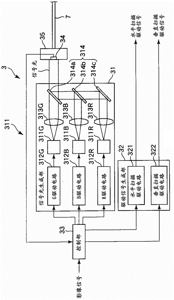
[0129] The aforementioned light sources 311R, 311G, and 311B are each constituted by an embodiment of the light emitting device of the present invention.
[0130] Figure 6 The illustrated light emitting device 9 includes a light emitting element 91 , a temperature variable resistance element 92 , a mount 93 , and a mounting substrate 94 .
[0131] Additionally, if Figure 7 As shown, the light emitting element 91...
no. 2 approach 》
[0168] Next, a second embodiment of the light emitting device of the present invention will be described.
[0169] Figure 9It is a perspective view showing the second embodiment of the light emitting device of the present invention.
[0170] Hereinafter, the second embodiment will be described. In the following description, differences from the above-mentioned first embodiment will be mainly described, and descriptions of the same items will be omitted. In addition, in the figure, the same code|symbol is attached|subjected to the same structure as the said embodiment. In addition, in Figure 9 In , illustration of the mounting substrate 94 is omitted.
[0171] The second embodiment is the same as the first embodiment except that the shape of the temperature variable resistance element 92 is different.
[0172] Such as Figure 9 As shown, the temperature variable resistance element 92 according to the second embodiment has a planar shape in which the terminal electrode 92...
no. 3 approach 》
[0179] Next, a third embodiment of the light emitting device of the present invention will be described.
[0180] Figure 10 It is a perspective view showing a third embodiment of the light emitting device of the present invention.
[0181] Hereinafter, the third embodiment will be described, and in the following description, the differences from the first and second embodiments described above will be mainly described, and the description of the same matters will be omitted. In addition, in the figure, the same code|symbol is attached|subjected to the same structure as the said embodiment. In addition, in Figure 10 In , illustration of the mounting substrate 94 is omitted.
[0182] The third embodiment is also the same as the second embodiment except that the shape of the temperature variable resistance element 92 is different.
[0183] Such as Figure 10 As shown, the temperature variable resistance element 92 according to the third embodiment has a planar shape in whi...
PUM
 Abstract
Description
Claims
Application Information


