Method for testing abnormal screen defect of LCD
A technology of abnormal defects and testing methods, applied in nonlinear optics, instruments, optics, etc., can solve problems such as high customer complaints and increased product maintenance costs, and achieve the effect of improving product reliability.
- Summary
- Abstract
- Description
- Claims
- Application Information
AI Technical Summary
Problems solved by technology
Method used
Image

Examples
Embodiment Construction
[0027] In order to further illustrate the principle and structure of the present invention, preferred embodiments of the present invention are now described in detail.
[0028] In this embodiment, the LCD designed and produced by a certain LCD manufacturer is tested to find out whether the LCD products produced by it have PCB connection defects, which will cause abnormalities such as poor contact or shedding of the PCB after long-term use of the LCD, resulting in a decrease in the performance of the LCD product or even unable to work properly.
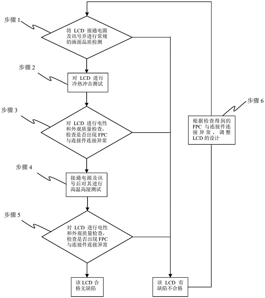
[0029] Such as figure 1 As shown, the method for testing the abnormal defect of the LCD screen of the present embodiment comprises the following steps:
[0030] Step 1, connect the LCD to be tested with power and signal and perform routine picture quality inspection. For the LCD to be tested in this step, 3 LCD product samples are randomly selected from the LCD products produced according to the time sequence of LCD production by the...
PUM
 Abstract
Description
Claims
Application Information