Method for controlling positioning precision of PCB drill holes

A technology of PCB board and positioning accuracy, applied in metal processing and other directions, can solve problems such as scrap, cannot be found in time, and have partial holes, and achieve the effect of good feasibility, simple design, and easy monitoring.

Active Publication Date: 2015-04-22
大连崇达电子有限公司
View PDF6 Cites 13 Cited by
  • Summary
  • Abstract
  • Description
  • Claims
  • Application Information

AI Technical Summary

Problems solved by technology

[0002] The types of PCB mechanical drilling in the industry include mechanical blind holes, through holes, VIA-in- p ad, back-drilling, etc., may involve one type or multiple types in one product. Boards with various drilling types need to be manufactured separately, because the board will expand and shrink during the manufacturing process, and the positioning of each drilling hole The method may also be different. It is difficult to ensure that each type of hole is drilled at the exact position required; however, there is an error in the position of each hole, and this error cannot be found in time during production, which will cause the product to be etched in the subsequent process. There is a phenomenon of partial hole in the back, which will lead to scrapping in severe cases

Method used


Image

  • Method for controlling positioning precision of PCB drill holes
  • Method for controlling positioning precision of PCB drill holes
  • Method for controlling positioning precision of PCB drill holes

Examples


Embodiment

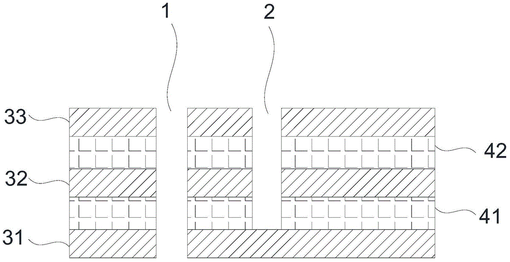
[0022] like figure 1 The shown PCB board includes the first PP layer 31, the first core board 41, the second PP layer 32, the second core board 42, and the third PP layer 33 stacked in sequence. It is necessary to make through holes 1 and 3 on the PCB board. The blind holes 2 from the first core board 41 to the third PP layer 33 . The production steps are as follows:

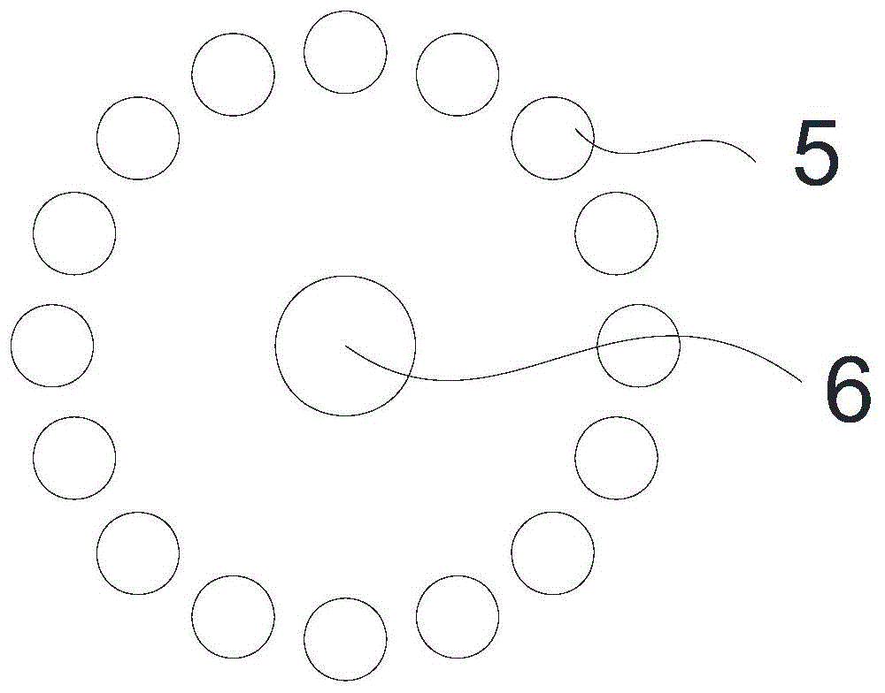
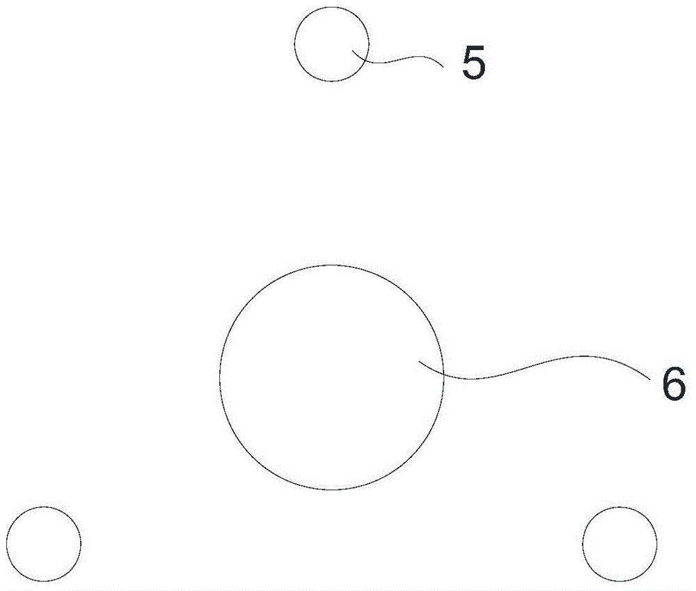
[0023] Drill holes at the positions where blind holes 2 need to be drilled on the laminated first core board 41 to the third PP layer 33, and then drill a series of equal-sized marked holes at the four corners of the laminated board without wiring 5. The diameter of the marking hole is 0.5mm; the marking holes 5 are arranged in a circular pattern of inspection modules (such as figure 2 ), the distance from hole to hole is 0.4mm.

[0024] After pressing the above-mentioned laminated board and the first PP layer 31 into a PCB board, reposition the position of the PCB board on the drilling machine; adjust the d...


PUM


Abstract

The invention discloses a method for controlling positioning precision of PCB drill holes, and belongs to the field of machining of the PCB drill holes. The method for controlling the positioning precision of the PCB drill holes comprises the following steps that a series of marking holes with the same size are drilled in non-wire-arrangement positions on a PCB to form one or more check module patterns; the position of the PCB on a drilling machine is repositioned, and a drill bit is adjusted to the set center positions of the check module patterns for drilling comparison holes; whether the comparison holes are positioned in the center positions of the checking module patterns is detected; the position of the PCB is adjusted or maintained to allow the drilled comparison holes to be positioned in the centers of the check module patterns; and a second drill hole is drilled in the PCB according to the set position coordinates of the second drill hole. The method disclosed in the technical scheme can prevent the hole deflection problem of two or more different positioning drill holes in the PCB due to such factors as expansion and shrinkage, different machining modes or separated production in the manufacturing process, and can reduce the waste of manpower and material costs because plates with deflected holes generated by multiple sets of positioning modes flow to a next process in the prior art.

Description

technical field [0001] The invention belongs to the field of PCB board drilling processing, and in particular relates to a method for controlling the positioning accuracy of PCB board drilling. Background technique [0002] The types of PCB mechanical drilling in the industry include mechanical blind holes, through holes, VIA-in- p ad, back-drilling, etc., may involve one type or multiple types in one product. Boards with various drilling types need to be manufactured separately, because the board will expand and shrink during the manufacturing process, and the positioning of each drilling hole The method may also be different. It is difficult to ensure that each type of hole is drilled in the exact position required; however, there is an error in the position of each hole, and this error cannot be found in time during production, which will cause the product to be etched in the subsequent process. There is a phenomenon of partial hole at the end, which will lead to scrappi...

Claims


Application Information

Patent Timeline
Patent Type & Authority Applications(China)
IPC IPC(8): B26F1/16
CPCB26F1/16
Inventor 黄海蛟翟青霞朱拓王淑怡
Owner 大连崇达电子有限公司
Why Eureka
Try Eureka