An organic light emitting diode display panel, a method for making the same, and a display device

A technology of light-emitting diodes and display panels, applied in semiconductor/solid-state device manufacturing, electrical components, electric solid-state devices, etc., can solve the problems of complex process steps, many times of patterning and etching, and high cost, so as to reduce process steps, The effect of reducing production cost and quantity

Active Publication Date: 2018-04-10
BOE TECH GRP CO LTD
View PDF4 Cites 0 Cited by
  • Summary
  • Abstract
  • Description
  • Claims
  • Application Information

AI Technical Summary

Problems solved by technology

[0005] To sum up, in the manufacturing process of organic light-emitting diode display panels in the prior art, the whole process needs to be completed by using six masks, and the number of patterning and etching in the manufacturing process is many, the process steps are complicated, and the cost is high.

Method used


Image

  • An organic light emitting diode display panel, a method for making the same, and a display device
  • An organic light emitting diode display panel, a method for making the same, and a display device
  • An organic light emitting diode display panel, a method for making the same, and a display device

Examples


Embodiment Construction

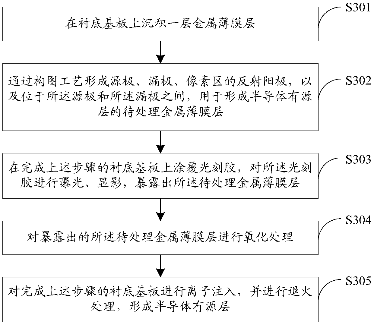
[0034] Embodiments of the present invention provide an organic light emitting diode display panel, a manufacturing method thereof, and a display device, so as to reduce process steps and reduce production costs.

[0035] In order to make the purpose, technical solutions and advantages of the present invention clearer, the present invention will be further described in detail below in conjunction with the accompanying drawings. Obviously, the described embodiments are only some of the embodiments of the present invention, rather than all of them. Based on the embodiments of the present invention, all other embodiments obtained by persons of ordinary skill in the art without making creative efforts belong to the protection scope of the present invention.

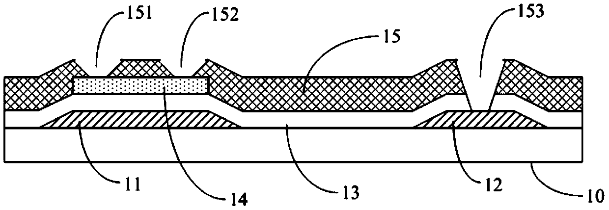
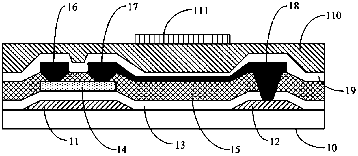
[0036] The organic light emitting diode display panel provided by the specific embodiments of the present invention and the manufacturing method thereof will be described in detail below with reference to the accompanying drawi...


PUM


Abstract

The invention discloses an organic light-emitting diode display panel, a manufacturing method thereof, and a display device, which are used for reducing process steps and reducing production costs. The method includes: depositing a metal thin film layer on a base substrate; forming a source, a drain, and a reflective anode in a pixel region through a patterning process; The to-be-processed metal thin film layer of the semiconductor active layer; coating photoresist on the base substrate that has completed the above steps, exposing and developing the photoresist, exposing the to-be-processed metal thin film layer; performing oxidation treatment on the metal thin film layer to be treated; performing ion implantation and annealing treatment on the base substrate that has completed the above steps to form a semiconductor active layer.

Description

technical field [0001] The invention relates to the field of display technology, in particular to an organic light emitting diode display panel, a manufacturing method thereof, and a display device. Background technique [0002] At present, organic light emitting diode (Organic Light Emitting Diode, OLED) flat panel display is developing towards the direction of large size and high resolution, high yield, low-cost mass production is gradually advancing in major companies, thin film transistor array technology (TFT Array) It plays a key role in the mass production of flat panel displays. Compared with amorphous silicon thin film transistor (ThinFilm Transistor, TFT), the carrier mobility of oxide TFT is as high as 10cm 2 / Vs is about 10 times that of the former; therefore, the mass production of oxide TFTs has become particularly important. In the process of mass production of the still immature oxide TFT backplane, reducing process steps and controlling costs have always ne...

Claims


Application Information

Patent Timeline
Patent Type & Authority Patents(China)
IPC IPC(8): H01L21/84H01L27/12H01L51/56H01L27/32
Inventor 刘威姜春生
Owner BOE TECH GRP CO LTD
Why Eureka
Try Eureka