Touch control board

A touch panel and substrate technology, which is applied in the fields of instruments, electrical digital data processing, and data processing input/output processes, etc., can solve the problems of unfavorable design trends in the surrounding area 142, and achieve the reduction of the area size, the realization of design, and the realization of narrower The effect of the border

Inactive Publication Date: 2015-06-17
WINTEK CORP
View PDF3 Cites 8 Cited by
  • Summary
  • Abstract
  • Description
  • Claims
  • Application Information

AI Technical Summary

Problems solved by technology

Since the line width and spacing of each first touch signal trace 120T are limited due to electrical requirements, when the touch resolution requirement of the capacitive touch panel 100 is increased, the first axial electrodes 120 and Therefore, the number of the second axial electrodes 130 will be increased, and the number of the first touch signal traces 120T will also be correspondingly increased, so that the surrounding area 142 must maintain a certain size, which is not conducive to improving the appearance and visual effect. The design trend of narrow borders on touchpads

Method used


Image

  • Touch control board
  • Touch control board
  • Touch control board

Examples


Embodiment 1

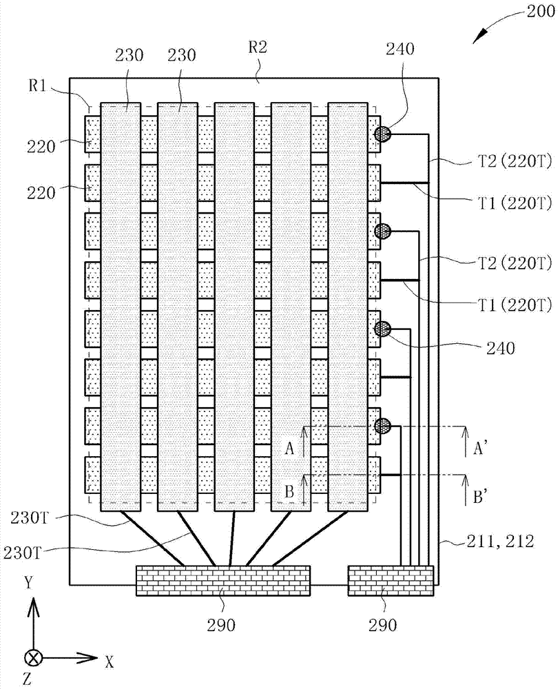
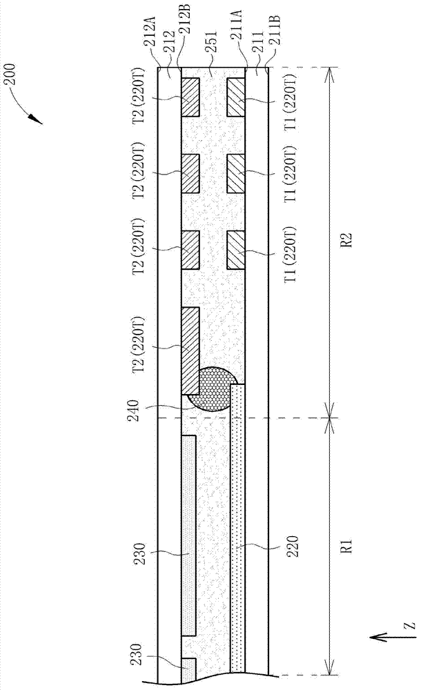
[0063] Such as Figure 2 to Figure 4 As shown, the touch panel 200 according to Embodiment 1 of the present invention has a light-transmitting region R1 and a surrounding region R2. The surrounding area R2 is located on at least one side of the transparent area R1. In this embodiment, the surrounding area R2 preferably surrounds the transparent area R1, but it is not limited thereto. The touch panel 200 includes a first base 211 , a second base 212 , a plurality of first electrodes 220 , at least one first trace T1 , at least one second trace T2 and at least one conductive structure 240 . The first base 211 has a first surface 211A and a second surface 211B, and the first surface 211A is opposite to the second surface 211B. The second base 212 is opposite to the first base 211 . The second substrate 212 has a third surface 212A and a fourth surface 212B, the fourth surface 212B is opposite to the third surface 212A, and the first surface 211A of the first substrate 211 face...

Embodiment 2

[0068] Such as Figure 5 As shown, the touch panel 300 according to Embodiment 2 of the present invention may further include a decoration layer 260 disposed between the first substrate 211 and the second substrate 212 and located in the surrounding area R2. In this embodiment, the decoration layer 260 is preferably disposed on the fourth surface 212B of the second substrate 212 and located between the second trace T2 and the second substrate 212 , but it is not limited thereto. In addition, the second substrate 212 of this embodiment is preferably a cover plate such as cover glass or cover plastic. The cover plate can be a light-transmitting substrate strengthened by chemical or physical methods, such as strengthened glass after chemical ion exchange or heat treatment, which has high mechanical strength, anti-fouling, anti-scratch and other characteristics, and can protect adjacent touch components Or a monitor. The decoration layer 260 can be used to form an appearance dec...

Embodiment 3

[0070] Such as Figure 6 to Figure 8 As shown, the difference between the touch panel 400 of the third embodiment of the present invention and the first embodiment above is that the first trace T1 and the second trace T1 respectively arranged on the first substrate 211 and the second substrate 212 in this embodiment The wires T2 are preferably arranged to be offset from each other, so as to reduce signal interference between each other. In this embodiment, there is a space area S between two adjacent first traces T1, and at least one second trace T2 and the corresponding space area S at least partially overlap each other in the vertical projection direction Z, for The overlapping area of ​​the first trace T1 and the second trace T2 in the vertical projection direction Z is reduced, thereby reducing the signal interference between the first trace T1 and the second trace T2. Specifically, the center point of the at least one second trace T2 in the first direction X preferably o...


PUM


Abstract

The invention discloses a touch control board, comprising a first substrate, a second substrate, a plurality of first electrodes, a first wiring, a second wiring and a conductive structure. The second substrate and the first substrate are oppositely arranged, and a first surface of the first substrate is facing a fourth surface of the second substrate. The first electrodes are arranged on the first surface of the first substrate and are at least partially positioned in a light transmitting area. The first wiring is arranged on the first surface of the first substrate and is at least partially positioned in a periphery area. The first wring is electrically connected with one of the plurality of the first electrodes. The second wiring is arranged on the fourth surface of the second substrate and is at least partially positioned in the periphery area. The second wiring is electrically connected with another of the plurality of first electrodes. The conductive structure is arranged between the first substrate and the second substrate. The second wiring is electrically connected with one of the plurality of first electrodes through the conductive structure. The wiring parts connected with the same electrode are arranged on another substrate, so that the size of the periphery area is reduced.

Description

technical field [0001] The invention relates to a touch panel, in particular to a touch panel in which the wiring part connected to the same sensing electrode is arranged on another substrate to reduce the surrounding area. Background technique [0002] The technology development of the touch panel is very diverse, and the more common technologies include resistive, capacitive and optical. Among them, the capacitive touch panel has become the mainstream touch technology used in mid-to-high-end consumer electronic products due to its characteristics of high accuracy, multi-touch, high durability, and high touch resolution. The operating principle of the capacitive touch panel is to use the sensing electrodes to detect the capacitance change of the touch points, and use the connecting wires connecting each electrode on the axis of different directions to transmit the signal back to complete the positioning. Such as figure 1 As shown, the existing capacitive touch panel 100 i...

Claims


Application Information

Patent Timeline
Patent Type & Authority Applications(China)
IPC IPC(8): G06F3/041G06F3/044
Inventor 徐荣瑞
Owner WINTEK CORP
Why Eureka
Try Eureka