Mask plate and encapsulating method for OLED device

A packaging method and mask technology, which are applied in the manufacturing of electric solid-state devices, semiconductor devices, semiconductor/solid-state devices, etc., can solve the problems of unfavorable narrow frame realization, intrusion, device failure, etc., and achieve narrow frame design and extended use. Longevity, the effect of improving the packaging effect

Active Publication Date: 2017-04-19
WUHAN CHINA STAR OPTOELECTRONICS SEMICON DISPLAY TECH CO LTD
View PDF4 Cites 23 Cited by
  • Summary
  • Abstract
  • Description
  • Claims
  • Application Information

AI Technical Summary

Problems solved by technology

see figure 1 When using CVD or ALD to form the passivation layer 2 on the substrate 1, the shadow effect (Shadow effect) is likely to occur at the edge of the passivation layer 2, that is, the inorganic material will continue to be deposited on the periphery of the set film-forming area, making the actual The film-forming area is larger than the set film-forming area, which is not conducive to the realization of narrow borders, and may cause water vapor and oxygen to invade from the area formed by the shadow effect, resulting in device failure

Method used


Image

  • Mask plate and encapsulating method for OLED device
  • Mask plate and encapsulating method for OLED device
  • Mask plate and encapsulating method for OLED device

Examples


Embodiment Construction

[0030] In order to further illustrate the technical means adopted by the present invention and its effects, the following describes in detail in conjunction with preferred embodiments of the present invention and accompanying drawings.

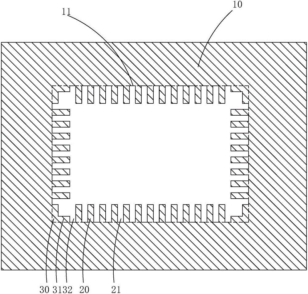
[0031] see figure 2 , the present invention provides a mask plate, comprising a frame body 10 and a plurality of rectangular shielding parts 20 arranged on the frame body 10; the frame body 10 has a rectangular opening 11, and the plurality of rectangular shielding parts 20 are uniformly arranged On the four sides of the rectangular opening 11, the rectangular shielding parts 20 on the same side all extend to the opposite side, and a second rectangular shielding part 20 is formed between two adjacent rectangular shielding parts 20 on the same side. A groove 21.

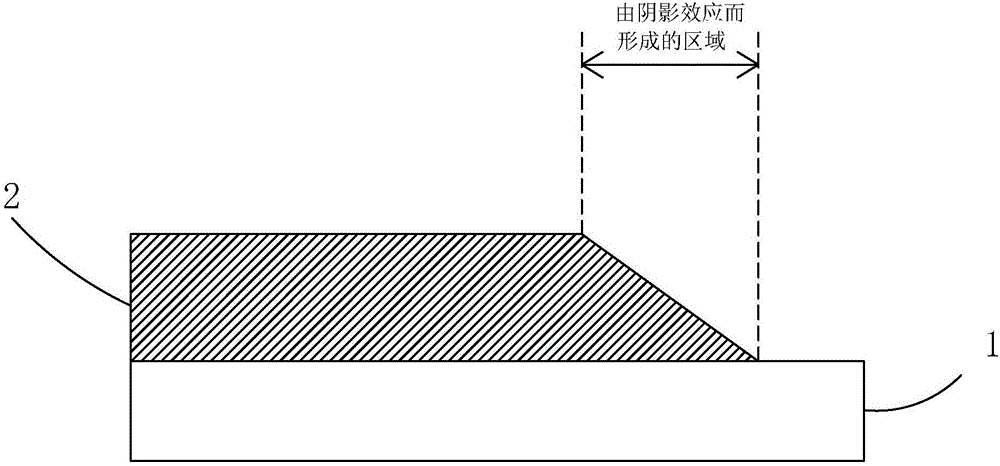
[0032]It should be noted that the mask plate of the present invention is used to deposit inorganic materials to form the passivation layer in the thin film encapsulation layer, and ...


PUM


Abstract

The invention provides a mask plate and an encapsulating method for an OLED device. According to the mask plate provided by the invention, a plurality of rectangular shielding parts are uniformly arranged on four sides of a rectangular opening of a frame body; when the mask plate is utilized to encapsulate the OLED device, three independent sides of the rectangular shielding parts generate shadow effects, so that film thickness of a passivation layer formed below the rectangular shielding parts is the same as that of a passivation layer formed below a residual un-shielded area in the rectangular opening; moreover, positions on which the rectangular shielding parts are connected with the sides of the rectangular opening do not generate shadow effects, and the shadow effect generated by a bottom side of a first groove between adjacent two rectangular shielding parts is diffused towards the positions on which the adjacent rectangular shielding parts are connected with the sides of the rectangular opening for being diluted and reduced, so that the shadow effects of the side integers of the rectangular opening is reduced, and an actual film-forming area of the passivation layer is almost the same as a preset designed film-forming layer, and therefore, a narrow side frame design can be realized, encapsulating effect is improved, and the service life of the device is prolonged.

Description

technical field [0001] The invention relates to the field of display technology, in particular to a mask plate and a packaging method for an OLED device. Background technique [0002] In recent years, flat panel display devices such as Liquid Crystal Display (LCD) devices and Organic Light Emitting Diode (OLED) display devices have gradually replaced CRT displays and become mainstream products in the display device market. Among them, OLED display devices have many advantages such as self-illumination, low driving voltage, high luminous efficiency, short response time, high definition and contrast, near 180° viewing angle, wide operating temperature range, flexible display and large-area full-color display, etc. , is recognized by the industry as the most promising display device. [0003] An OLED display device generally includes: a substrate, an encapsulation cover plate disposed opposite to the substrate, an anode disposed on the substrate, a hole injection layer dispose...

Claims


Application Information

Patent Timeline
Patent Type & Authority Applications(China)
IPC IPC(8): C23C16/04H01L51/52H01L51/56
CPCC23C16/042H10K50/84H10K71/00
Inventor 王杲祯余威
Owner WUHAN CHINA STAR OPTOELECTRONICS SEMICON DISPLAY TECH CO LTD
Why Eureka
Try Eureka